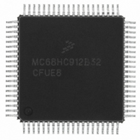
MCHC912B32CFUE8 Freescale Semiconductor, MCHC912B32CFUE8 Datasheet - Page 205

MCHC912B32CFUE8
Manufacturer Part Number
MCHC912B32CFUE8
Description
IC MCU 32K FLASH 8MHZ 80-QFP
Manufacturer
Freescale Semiconductor
Series
HC12r
Datasheet
1.MCHC912B32CFUE8.pdf
(334 pages)
Specifications of MCHC912B32CFUE8
Core Processor
CPU12
Core Size
16-Bit
Speed
8MHz
Connectivity
SCI, SPI
Peripherals
POR, PWM, WDT
Number Of I /o
63
Program Memory Size
32KB (32K x 8)
Program Memory Type
FLASH
Eeprom Size
768 x 8
Ram Size
1K x 8
Voltage - Supply (vcc/vdd)
4.5 V ~ 5.5 V
Data Converters
A/D 8x10b
Oscillator Type
External
Operating Temperature
-40°C ~ 85°C
Package / Case
80-QFP
Cpu Family
HC12
Device Core Size
16b
Frequency (max)
8MHz
Interface Type
SCI/SPI
Total Internal Ram Size
1KB
# I/os (max)
63
Operating Supply Voltage (typ)
5V
Operating Supply Voltage (max)
5.5V
Operating Supply Voltage (min)
4.5V
On-chip Adc
8-chx10-bit
Instruction Set Architecture
CISC
Operating Temp Range
-40C to 85C
Operating Temperature Classification
Industrial
Mounting
Surface Mount
Pin Count
80
Package Type
PQFP
Package
80PQFP
Family Name
HC12
Maximum Speed
8 MHz
Operating Supply Voltage
5 V
Data Bus Width
16 Bit
Number Of Programmable I/os
63
Processor Series
HC912B
Core
HC12
Data Ram Size
1 KB
Maximum Clock Frequency
8 MHz
Maximum Operating Temperature
+ 85 C
Mounting Style
SMD/SMT
3rd Party Development Tools
EWHCS12
Development Tools By Supplier
M68EVB912B32E
Minimum Operating Temperature
- 40 C
Lead Free Status / RoHS Status
Lead free / RoHS Compliant
Available stocks
Company
Part Number
Manufacturer
Quantity
Price
Company:
Part Number:
MCHC912B32CFUE8
Manufacturer:
Freescale Semiconductor
Quantity:
10 000
- Current page: 205 of 334
- Download datasheet (2Mb)
SPE — SPI System Enable Bit
SWOM — Port S Wired-OR Mode Bit
MSTR — SPI Master/Slave Mode Select Bit
CPOL and CPHA — SPI Clock Polarity, Clock Phase Bits
SSOE — Slave Select Output Enable Bit
LSBF — SPI LSB First Enable Bit
14.3.5.2 SPI Control Register 2
Read: Anytime
Write: Anytime
PUPS — Pullup Port S Enable Bit
RDS — Reduce Drive of Port S Bit
Freescale Semiconductor
When MODF is set, SPE always reads 0. SP0CR1 must be written as part of a mode fault recovery
sequence.
Controls not only SPI output pins but also the general-purpose output pins (PS4–PS7) which are not
used by SPI.
These two bits are used to specify the clock format to be used in SPI operations. When the clock
polarity bit is cleared and data is not being transferred, the SCK pin of the master device is low. When
CPOL is set, SCK idles high. See
The SS output feature is enabled only in master mode by asserting the SSOE and DDS7.
Normally, data is transferred MSB first. This bit does not affect the position of the MSB and LSB in the
data register. Reads and writes of the data register always have MSB in bit 7.
0 = SPI internal hardware is initialized and SPI system is in a low-power disabled state.
1 = PS4–PS7 are dedicated to the SPI function.
0 = SPI and/or PS4–PS7 output buffers operate normally.
1 = SPI and/or PS4–PS7 output buffers behave as open-drain outputs.
0 = Slave mode
1 = Master mode
0 = Data is transferred most-significant bit (MSB) first.
1 = Data is transferred least-significant bit (LSB) first.
0 = No internal pullups on port S
1 = All port S input pins have an active pullup device. If a pin is programmed as output, the pullup
0 = Port S output drivers operate normally.
1 = All port S output pins have reduced drive capability for lower power and less noise.
device becomes inactive.
Address:
Reset:
Read:
Write:
$00D1
Bit 7
0
0
Figure 14-16. SPI Control Register 2 (SP0CR2)
= Unimplemented
M68HC12B Family Data Sheet, Rev. 9.1
6
0
0
Figure 14-12
5
0
0
and
4
0
0
Figure
PUPS
14-13.
3
1
RDS
2
0
Serial Peripheral Interface (SPI)
1
0
0
SPC0
Bit 0
0
205
Related parts for MCHC912B32CFUE8
Image
Part Number
Description
Manufacturer
Datasheet
Request
R
Part Number:
Description:
Manufacturer:
Freescale Semiconductor, Inc
Datasheet:
Part Number:
Description:
Manufacturer:
Freescale Semiconductor, Inc
Datasheet:
Part Number:
Description:
Manufacturer:
Freescale Semiconductor, Inc
Datasheet:
Part Number:
Description:
Manufacturer:
Freescale Semiconductor, Inc
Datasheet:
Part Number:
Description:
Manufacturer:
Freescale Semiconductor, Inc
Datasheet:
Part Number:
Description:
Manufacturer:
Freescale Semiconductor, Inc
Datasheet:
Part Number:
Description:
Manufacturer:
Freescale Semiconductor, Inc
Datasheet:
Part Number:
Description:
Manufacturer:
Freescale Semiconductor, Inc
Datasheet:
Part Number:
Description:
Manufacturer:
Freescale Semiconductor, Inc
Datasheet:
Part Number:
Description:
Manufacturer:
Freescale Semiconductor, Inc
Datasheet:
Part Number:
Description:
Manufacturer:
Freescale Semiconductor, Inc
Datasheet:
Part Number:
Description:
Manufacturer:
Freescale Semiconductor, Inc
Datasheet:
Part Number:
Description:
Manufacturer:
Freescale Semiconductor, Inc
Datasheet:
Part Number:
Description:
Manufacturer:
Freescale Semiconductor, Inc
Datasheet:
Part Number:
Description:
Manufacturer:
Freescale Semiconductor, Inc
Datasheet:


