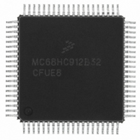
MCHC912B32CFUE8 Freescale Semiconductor, MCHC912B32CFUE8 Datasheet - Page 237

MCHC912B32CFUE8
Manufacturer Part Number
MCHC912B32CFUE8
Description
IC MCU 32K FLASH 8MHZ 80-QFP
Manufacturer
Freescale Semiconductor
Series
HC12r
Datasheet
1.MCHC912B32CFUE8.pdf
(334 pages)
Specifications of MCHC912B32CFUE8
Core Processor
CPU12
Core Size
16-Bit
Speed
8MHz
Connectivity
SCI, SPI
Peripherals
POR, PWM, WDT
Number Of I /o
63
Program Memory Size
32KB (32K x 8)
Program Memory Type
FLASH
Eeprom Size
768 x 8
Ram Size
1K x 8
Voltage - Supply (vcc/vdd)
4.5 V ~ 5.5 V
Data Converters
A/D 8x10b
Oscillator Type
External
Operating Temperature
-40°C ~ 85°C
Package / Case
80-QFP
Cpu Family
HC12
Device Core Size
16b
Frequency (max)
8MHz
Interface Type
SCI/SPI
Total Internal Ram Size
1KB
# I/os (max)
63
Operating Supply Voltage (typ)
5V
Operating Supply Voltage (max)
5.5V
Operating Supply Voltage (min)
4.5V
On-chip Adc
8-chx10-bit
Instruction Set Architecture
CISC
Operating Temp Range
-40C to 85C
Operating Temperature Classification
Industrial
Mounting
Surface Mount
Pin Count
80
Package Type
PQFP
Package
80PQFP
Family Name
HC12
Maximum Speed
8 MHz
Operating Supply Voltage
5 V
Data Bus Width
16 Bit
Number Of Programmable I/os
63
Processor Series
HC912B
Core
HC12
Data Ram Size
1 KB
Maximum Clock Frequency
8 MHz
Maximum Operating Temperature
+ 85 C
Mounting Style
SMD/SMT
3rd Party Development Tools
EWHCS12
Development Tools By Supplier
M68EVB912B32E
Minimum Operating Temperature
- 40 C
Lead Free Status / RoHS Status
Lead free / RoHS Compliant
Available stocks
Company
Part Number
Manufacturer
Quantity
Price
Company:
Part Number:
MCHC912B32CFUE8
Manufacturer:
Freescale Semiconductor
Quantity:
10 000
- Current page: 237 of 334
- Download datasheet (2Mb)
15.9.3 BDLC State Vector Register
This register is provided to substantially decrease the CPU overhead associated with servicing interrupts
while under operation of a multiplex protocol. It provides an index offset that is directly related to the
BDLC’s current state, which can be used with a user-supplied jump table to rapidly enter an interrupt
service routine. This eliminates the need for the user to maintain a duplicate state machine in software.
I0, I1, I2, I3 — Interrupt Source Bits
Freescale Semiconductor
If the TMIFR1 bit is set, the BDLC attempts to transmit the normalization symbol followed by the byte
in the BDR. After the byte in the BDR has been loaded into the transmit shift register, a TDRE interrupt
(see
programmer should then load the next byte of the IFR into the BDR for transmission. When the last
byte of the IFR has been loaded into the BDR, the programmer should set the TEOD bit in the BDLC
control register 2 (BCR2). This instructs the BDLC to transmit a CRC byte once the byte in the BDR is
transmitted, and then transmit an EOD symbol, indicating the end of the IFR portion of the message
frame.
However, to transmit a single byte followed by a CRC byte, the programmer should load the byte into
the BDR before the EOD symbol has been received, and then set the TMIFR1 bit. Once the TDRE
interrupt occurs, the programmer sets the TEOD bit in the BCR2. This results in the byte in the BDR
being the only byte transmitted before the IFR CRC byte, and no TDRE interrupt is generated.
If the programmer attempts to set the TMIFR1 bit immediately after the EOD symbol has been received
from the bus, the TMIFR1 bit remains in the reset state, and no attempt is made to transmit an IFR byte.
If a loss of arbitration occurs when the BDLC is transmitting any byte of a multiple byte IFR, the BDLC
goes to the loss of arbitration state, sets the appropriate flag, and ceases transmission.
If the BDLC loses arbitration during the IFR, the TMIFR1 bit is cleared and no attempt is made to
retransmit the byte in the BDR. If loss of arbitration occurs in the last bit of the IFR byte, two additional
1 bits are sent out.
These bits indicate the source of the pending interrupt request. Bits are encoded according to
15-4.
15.9.3 BDLC State Vector
Address: $00F9
The extra logic 1 bits are an enhancement to the J1850 protocol which
forces a byte boundary condition fault. This is helpful in preventing noise on
the J1850 bus from corrupting a message.
Reset:
Read:
Write:
Bit 7
Figure 15-15. BDLC State Vector Register (BSVR)
0
0
= Unimplemented
Register) occurs similar to the main message transmit sequence. The
M68HC12B Family Data Sheet, Rev. 9.1
6
0
0
I3
5
0
NOTE
I2
4
0
I1
3
0
I0
2
0
1
0
0
Bit 0
0
0
BDLC Registers
Table
237
Related parts for MCHC912B32CFUE8
Image
Part Number
Description
Manufacturer
Datasheet
Request
R
Part Number:
Description:
Manufacturer:
Freescale Semiconductor, Inc
Datasheet:
Part Number:
Description:
Manufacturer:
Freescale Semiconductor, Inc
Datasheet:
Part Number:
Description:
Manufacturer:
Freescale Semiconductor, Inc
Datasheet:
Part Number:
Description:
Manufacturer:
Freescale Semiconductor, Inc
Datasheet:
Part Number:
Description:
Manufacturer:
Freescale Semiconductor, Inc
Datasheet:
Part Number:
Description:
Manufacturer:
Freescale Semiconductor, Inc
Datasheet:
Part Number:
Description:
Manufacturer:
Freescale Semiconductor, Inc
Datasheet:
Part Number:
Description:
Manufacturer:
Freescale Semiconductor, Inc
Datasheet:
Part Number:
Description:
Manufacturer:
Freescale Semiconductor, Inc
Datasheet:
Part Number:
Description:
Manufacturer:
Freescale Semiconductor, Inc
Datasheet:
Part Number:
Description:
Manufacturer:
Freescale Semiconductor, Inc
Datasheet:
Part Number:
Description:
Manufacturer:
Freescale Semiconductor, Inc
Datasheet:
Part Number:
Description:
Manufacturer:
Freescale Semiconductor, Inc
Datasheet:
Part Number:
Description:
Manufacturer:
Freescale Semiconductor, Inc
Datasheet:
Part Number:
Description:
Manufacturer:
Freescale Semiconductor, Inc
Datasheet:


