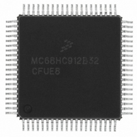
MCHC912B32CFUE8 Freescale Semiconductor, MCHC912B32CFUE8 Datasheet - Page 229

MCHC912B32CFUE8
Manufacturer Part Number
MCHC912B32CFUE8
Description
IC MCU 32K FLASH 8MHZ 80-QFP
Manufacturer
Freescale Semiconductor
Series
HC12r
Datasheet
1.MCHC912B32CFUE8.pdf
(334 pages)
Specifications of MCHC912B32CFUE8
Core Processor
CPU12
Core Size
16-Bit
Speed
8MHz
Connectivity
SCI, SPI
Peripherals
POR, PWM, WDT
Number Of I /o
63
Program Memory Size
32KB (32K x 8)
Program Memory Type
FLASH
Eeprom Size
768 x 8
Ram Size
1K x 8
Voltage - Supply (vcc/vdd)
4.5 V ~ 5.5 V
Data Converters
A/D 8x10b
Oscillator Type
External
Operating Temperature
-40°C ~ 85°C
Package / Case
80-QFP
Cpu Family
HC12
Device Core Size
16b
Frequency (max)
8MHz
Interface Type
SCI/SPI
Total Internal Ram Size
1KB
# I/os (max)
63
Operating Supply Voltage (typ)
5V
Operating Supply Voltage (max)
5.5V
Operating Supply Voltage (min)
4.5V
On-chip Adc
8-chx10-bit
Instruction Set Architecture
CISC
Operating Temp Range
-40C to 85C
Operating Temperature Classification
Industrial
Mounting
Surface Mount
Pin Count
80
Package Type
PQFP
Package
80PQFP
Family Name
HC12
Maximum Speed
8 MHz
Operating Supply Voltage
5 V
Data Bus Width
16 Bit
Number Of Programmable I/os
63
Processor Series
HC912B
Core
HC12
Data Ram Size
1 KB
Maximum Clock Frequency
8 MHz
Maximum Operating Temperature
+ 85 C
Mounting Style
SMD/SMT
3rd Party Development Tools
EWHCS12
Development Tools By Supplier
M68EVB912B32E
Minimum Operating Temperature
- 40 C
Lead Free Status / RoHS Status
Lead free / RoHS Compliant
Available stocks
Company
Part Number
Manufacturer
Quantity
Price
Company:
Part Number:
MCHC912B32CFUE8
Manufacturer:
Freescale Semiconductor
Quantity:
10 000
- Current page: 229 of 334
- Download datasheet (2Mb)
Once the Tx shift register has completed its shifting operation for the current byte, the data byte in the Tx
shadow register is loaded into the Tx shift register. After this transfer takes place, the Tx shadow register
is ready to accept new data from the CPU when the TDRE flag in the BSVR is set.
15.8.4 Digital Loopback Multiplexer
The digital loopback multiplexer connects RxD to either BDTxD or BDRxD, depending on the state of the
DLOOP bit in the BCR2. (See
15.8.5 State Machine
All functions associated with performing the protocol are executed or controlled by the state machine. The
state machine is responsible for framing, collision detection, arbitration, CRC generation/checking, and
error detection. These sections describe the BDLC’s actions in a variety of situations.
15.8.5.1 4X Mode
The BDLC can exist on the same J1850 bus as modules which use a special 4X (41.6 Kbps) mode of
J1850 variable pulse width modulation (VPW) operation. The BDLC cannot transmit in 4X mode, but it
can receive messages in 4X mode, if the RX4X bit is set in BCR2. If the RX4X bit is not set in the BCR2,
any 4X message on the J1850 bus is treated as noise by the BDLC and is ignored.
15.8.5.2 Receiving a Message in Block Mode
Although not a part of the SAE J1850 protocol, the BDLC does allow for a special block mode of operation
of the receiver. As far as the BDLC is concerned, a block mode message is simply a long J1850 frame
Freescale Semiconductor
DLOOP FROM BCR2
LOOPBACK CONTROL
Figure 15-11. BDLC Protocol Handler Outline
15.9.2 BDLC Control Register
M68HC12B Family Data Sheet, Rev. 9.1
Rx SHADOW REGISTER
Rx SHIFT REGISTER
BDRxD
MULTIPLEXER
LOOPBACK
8
TO CPU INTERFACE AND Rx/Tx BUFFERS
TO PHYSICAL INTERFACE
STATE MACHINE
BDTxD
2.)
Tx SHADOW REGISTER
Tx SHIFT REGISTER
8
BDLC Protocol Handler
229
Related parts for MCHC912B32CFUE8
Image
Part Number
Description
Manufacturer
Datasheet
Request
R
Part Number:
Description:
Manufacturer:
Freescale Semiconductor, Inc
Datasheet:
Part Number:
Description:
Manufacturer:
Freescale Semiconductor, Inc
Datasheet:
Part Number:
Description:
Manufacturer:
Freescale Semiconductor, Inc
Datasheet:
Part Number:
Description:
Manufacturer:
Freescale Semiconductor, Inc
Datasheet:
Part Number:
Description:
Manufacturer:
Freescale Semiconductor, Inc
Datasheet:
Part Number:
Description:
Manufacturer:
Freescale Semiconductor, Inc
Datasheet:
Part Number:
Description:
Manufacturer:
Freescale Semiconductor, Inc
Datasheet:
Part Number:
Description:
Manufacturer:
Freescale Semiconductor, Inc
Datasheet:
Part Number:
Description:
Manufacturer:
Freescale Semiconductor, Inc
Datasheet:
Part Number:
Description:
Manufacturer:
Freescale Semiconductor, Inc
Datasheet:
Part Number:
Description:
Manufacturer:
Freescale Semiconductor, Inc
Datasheet:
Part Number:
Description:
Manufacturer:
Freescale Semiconductor, Inc
Datasheet:
Part Number:
Description:
Manufacturer:
Freescale Semiconductor, Inc
Datasheet:
Part Number:
Description:
Manufacturer:
Freescale Semiconductor, Inc
Datasheet:
Part Number:
Description:
Manufacturer:
Freescale Semiconductor, Inc
Datasheet:


