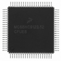
MCHC912B32CFUE8 Freescale Semiconductor, MCHC912B32CFUE8 Datasheet - Page 218

MCHC912B32CFUE8
Manufacturer Part Number
MCHC912B32CFUE8
Description
IC MCU 32K FLASH 8MHZ 80-QFP
Manufacturer
Freescale Semiconductor
Series
HC12r
Datasheet
1.MCHC912B32CFUE8.pdf
(334 pages)
Specifications of MCHC912B32CFUE8
Core Processor
CPU12
Core Size
16-Bit
Speed
8MHz
Connectivity
SCI, SPI
Peripherals
POR, PWM, WDT
Number Of I /o
63
Program Memory Size
32KB (32K x 8)
Program Memory Type
FLASH
Eeprom Size
768 x 8
Ram Size
1K x 8
Voltage - Supply (vcc/vdd)
4.5 V ~ 5.5 V
Data Converters
A/D 8x10b
Oscillator Type
External
Operating Temperature
-40°C ~ 85°C
Package / Case
80-QFP
Cpu Family
HC12
Device Core Size
16b
Frequency (max)
8MHz
Interface Type
SCI/SPI
Total Internal Ram Size
1KB
# I/os (max)
63
Operating Supply Voltage (typ)
5V
Operating Supply Voltage (max)
5.5V
Operating Supply Voltage (min)
4.5V
On-chip Adc
8-chx10-bit
Instruction Set Architecture
CISC
Operating Temp Range
-40C to 85C
Operating Temperature Classification
Industrial
Mounting
Surface Mount
Pin Count
80
Package Type
PQFP
Package
80PQFP
Family Name
HC12
Maximum Speed
8 MHz
Operating Supply Voltage
5 V
Data Bus Width
16 Bit
Number Of Programmable I/os
63
Processor Series
HC912B
Core
HC12
Data Ram Size
1 KB
Maximum Clock Frequency
8 MHz
Maximum Operating Temperature
+ 85 C
Mounting Style
SMD/SMT
3rd Party Development Tools
EWHCS12
Development Tools By Supplier
M68EVB912B32E
Minimum Operating Temperature
- 40 C
Lead Free Status / RoHS Status
Lead free / RoHS Compliant
Available stocks
Company
Part Number
Manufacturer
Quantity
Price
Company:
Part Number:
MCHC912B32CFUE8
Manufacturer:
Freescale Semiconductor
Quantity:
10 000
- Current page: 218 of 334
- Download datasheet (2Mb)
Byte Data Link Communications (BDLC)
15.7 BDLC MUX Interface
The MUX (multiplex) interface is responsible for bit encoding/decoding and digital noise filtering between
the protocol handler and the physical interface.
15.7.1 Rx Digital Filter
The receiver section of the BDLC includes a digital low-pass filter to remove narrow noise pulses from the
incoming message. An outline of the digital filter is shown in
Figure
15-3.
DATA
INPUT
4-BIT UP/DOWN COUNTER
LATCH
SYNC
RX DATA
FILTERED
FROM
RX DATA OUT
PHYSICAL
D
Q
UP/DOWN
OUT
D
Q
INTERFACE
(BDRXD)
MUX
INTERFACE
CLOCK
Figure 15-3. BDLC Rx Digital Filter Block Diagram
15.7.1.1 Operation
The clock for the digital filter is provided by the MUX interface clock (see f
parameter in
Table
15-2).
BDLC
At each positive edge of the clock signal, the current state of the receiver physical interface (BDRxD)
signal is sampled. The BDRxD signal state is used to determine whether the counter should increment or
decrement at the next negative edge of the clock signal.
The counter increments if the input data sample is high but decrements if the input sample is low.
Therefore, the counter progresses either up toward 15 if, on average, the BDRxD signal remains high or
progresses down toward 0 if, on average, the BDRxD signal remains low.
When the counter eventually reaches the value 15, the digital filter decides that the condition of the
BDRxD signal is at a stable logic level 1 and the data latch is set, causing the filtered Rx data signal to
become a logic level 1. Furthermore, the counter is prevented from overflowing and can be decremented
only from this state.
Alternatively, should the counter eventually reach the value 0, the digital filter decides that the condition
of the BDRxD signal is at a stable logic level 0 and the data latch is reset, causing the filtered Rx data
signal to become a logic level 0. Furthermore, the counter is prevented from underflowing and can be
incremented only from this state.
The data latch retains its value until the counter next reaches the opposite end point, signifying a definite
transition of the signal.
M68HC12B Family Data Sheet, Rev. 9.1
218
Freescale Semiconductor
Related parts for MCHC912B32CFUE8
Image
Part Number
Description
Manufacturer
Datasheet
Request
R
Part Number:
Description:
Manufacturer:
Freescale Semiconductor, Inc
Datasheet:
Part Number:
Description:
Manufacturer:
Freescale Semiconductor, Inc
Datasheet:
Part Number:
Description:
Manufacturer:
Freescale Semiconductor, Inc
Datasheet:
Part Number:
Description:
Manufacturer:
Freescale Semiconductor, Inc
Datasheet:
Part Number:
Description:
Manufacturer:
Freescale Semiconductor, Inc
Datasheet:
Part Number:
Description:
Manufacturer:
Freescale Semiconductor, Inc
Datasheet:
Part Number:
Description:
Manufacturer:
Freescale Semiconductor, Inc
Datasheet:
Part Number:
Description:
Manufacturer:
Freescale Semiconductor, Inc
Datasheet:
Part Number:
Description:
Manufacturer:
Freescale Semiconductor, Inc
Datasheet:
Part Number:
Description:
Manufacturer:
Freescale Semiconductor, Inc
Datasheet:
Part Number:
Description:
Manufacturer:
Freescale Semiconductor, Inc
Datasheet:
Part Number:
Description:
Manufacturer:
Freescale Semiconductor, Inc
Datasheet:
Part Number:
Description:
Manufacturer:
Freescale Semiconductor, Inc
Datasheet:
Part Number:
Description:
Manufacturer:
Freescale Semiconductor, Inc
Datasheet:
Part Number:
Description:
Manufacturer:
Freescale Semiconductor, Inc
Datasheet:


