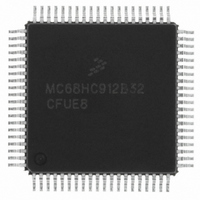
MCHC912B32CFUE8 Freescale Semiconductor, MCHC912B32CFUE8 Datasheet - Page 85

MCHC912B32CFUE8
Manufacturer Part Number
MCHC912B32CFUE8
Description
IC MCU 32K FLASH 8MHZ 80-QFP
Manufacturer
Freescale Semiconductor
Series
HC12r
Datasheet
1.MCHC912B32CFUE8.pdf
(334 pages)
Specifications of MCHC912B32CFUE8
Core Processor
CPU12
Core Size
16-Bit
Speed
8MHz
Connectivity
SCI, SPI
Peripherals
POR, PWM, WDT
Number Of I /o
63
Program Memory Size
32KB (32K x 8)
Program Memory Type
FLASH
Eeprom Size
768 x 8
Ram Size
1K x 8
Voltage - Supply (vcc/vdd)
4.5 V ~ 5.5 V
Data Converters
A/D 8x10b
Oscillator Type
External
Operating Temperature
-40°C ~ 85°C
Package / Case
80-QFP
Cpu Family
HC12
Device Core Size
16b
Frequency (max)
8MHz
Interface Type
SCI/SPI
Total Internal Ram Size
1KB
# I/os (max)
63
Operating Supply Voltage (typ)
5V
Operating Supply Voltage (max)
5.5V
Operating Supply Voltage (min)
4.5V
On-chip Adc
8-chx10-bit
Instruction Set Architecture
CISC
Operating Temp Range
-40C to 85C
Operating Temperature Classification
Industrial
Mounting
Surface Mount
Pin Count
80
Package Type
PQFP
Package
80PQFP
Family Name
HC12
Maximum Speed
8 MHz
Operating Supply Voltage
5 V
Data Bus Width
16 Bit
Number Of Programmable I/os
63
Processor Series
HC912B
Core
HC12
Data Ram Size
1 KB
Maximum Clock Frequency
8 MHz
Maximum Operating Temperature
+ 85 C
Mounting Style
SMD/SMT
3rd Party Development Tools
EWHCS12
Development Tools By Supplier
M68EVB912B32E
Minimum Operating Temperature
- 40 C
Lead Free Status / RoHS Status
Lead free / RoHS Compliant
Available stocks
Company
Part Number
Manufacturer
Quantity
Price
Company:
Part Number:
MCHC912B32CFUE8
Manufacturer:
Freescale Semiconductor
Quantity:
10 000
- Current page: 85 of 334
- Download datasheet (2Mb)
Chapter 6
Bus Control and Input/Output (I/O)
6.1 Introduction
Internally, the MCU has full 16-bit data paths, but depending upon the operating mode and control
registers, the external bus may be eight or 16 bits. There are cases where 8-bit and 16-bit accesses can
appear on adjacent cycles using the LSTRB signal to indicate 8-bit or 16-bit data.
6.2 Detecting Access Type from External Signals
The external signals LSTRB, R/W, and A0 can be used to determine the type of bus access that is taking
place. Accesses to the internal RAM module are the only accesses that produce LSTRB = A0 = 1,
because the internal RAM is specifically designed to allow misaligned 16-bit accesses in a single cycle.
In these cases, the data for the address that was accessed is on the low half of the data bus and the data
for address +1 is on the high half of the data bus (data order is swapped).
6.3 Registers
Under certain conditions, not all registers are visible in the memory map. In special peripheral mode, the
first 16 registers associated with bus expansion are removed from the memory map.
In expanded modes, some or all of port A, port B, and port E are used for expansion buses and control
signals. To allow emulation of the single-chip functions of these ports, some of these registers must be
rebuilt in an external port replacement unit. In any expanded mode,
port A and port B are used for address and data lines so registers for these ports, as well as the data
direction registers for these ports, are removed from the on-chip memory map and become external
accesses.
In any expanded mode, port E pins may be needed for bus control (for example, ECLK and R/W). To
regain the single-chip functions of port E, the emulate port E (EME) control bit in the MODE register may
Freescale Semiconductor
LSTRB
1
0
1
0
0
1
0
1
A0
0
1
0
1
0
1
0
1
R/W
1
1
0
0
1
1
0
0
Table 6-1. Detecting Access Type
M68HC12B Family Data Sheet, Rev. 9.1
8-bit read of an even address
8-bit read of an odd address
8-bit write to an even address
8-bit write to an odd address
16-bit read of an even address
16-bit read of an odd address (low/high data swapped)
16-bit write to an even address
16-bit write to an odd address (low/high data swapped)
Type of Access
85
Related parts for MCHC912B32CFUE8
Image
Part Number
Description
Manufacturer
Datasheet
Request
R
Part Number:
Description:
Manufacturer:
Freescale Semiconductor, Inc
Datasheet:
Part Number:
Description:
Manufacturer:
Freescale Semiconductor, Inc
Datasheet:
Part Number:
Description:
Manufacturer:
Freescale Semiconductor, Inc
Datasheet:
Part Number:
Description:
Manufacturer:
Freescale Semiconductor, Inc
Datasheet:
Part Number:
Description:
Manufacturer:
Freescale Semiconductor, Inc
Datasheet:
Part Number:
Description:
Manufacturer:
Freescale Semiconductor, Inc
Datasheet:
Part Number:
Description:
Manufacturer:
Freescale Semiconductor, Inc
Datasheet:
Part Number:
Description:
Manufacturer:
Freescale Semiconductor, Inc
Datasheet:
Part Number:
Description:
Manufacturer:
Freescale Semiconductor, Inc
Datasheet:
Part Number:
Description:
Manufacturer:
Freescale Semiconductor, Inc
Datasheet:
Part Number:
Description:
Manufacturer:
Freescale Semiconductor, Inc
Datasheet:
Part Number:
Description:
Manufacturer:
Freescale Semiconductor, Inc
Datasheet:
Part Number:
Description:
Manufacturer:
Freescale Semiconductor, Inc
Datasheet:
Part Number:
Description:
Manufacturer:
Freescale Semiconductor, Inc
Datasheet:
Part Number:
Description:
Manufacturer:
Freescale Semiconductor, Inc
Datasheet:


