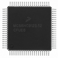
MCHC912B32CFUE8 Freescale Semiconductor, MCHC912B32CFUE8 Datasheet - Page 100

MCHC912B32CFUE8
Manufacturer Part Number
MCHC912B32CFUE8
Description
IC MCU 32K FLASH 8MHZ 80-QFP
Manufacturer
Freescale Semiconductor
Series
HC12r
Datasheet
1.MCHC912B32CFUE8.pdf
(334 pages)
Specifications of MCHC912B32CFUE8
Core Processor
CPU12
Core Size
16-Bit
Speed
8MHz
Connectivity
SCI, SPI
Peripherals
POR, PWM, WDT
Number Of I /o
63
Program Memory Size
32KB (32K x 8)
Program Memory Type
FLASH
Eeprom Size
768 x 8
Ram Size
1K x 8
Voltage - Supply (vcc/vdd)
4.5 V ~ 5.5 V
Data Converters
A/D 8x10b
Oscillator Type
External
Operating Temperature
-40°C ~ 85°C
Package / Case
80-QFP
Cpu Family
HC12
Device Core Size
16b
Frequency (max)
8MHz
Interface Type
SCI/SPI
Total Internal Ram Size
1KB
# I/os (max)
63
Operating Supply Voltage (typ)
5V
Operating Supply Voltage (max)
5.5V
Operating Supply Voltage (min)
4.5V
On-chip Adc
8-chx10-bit
Instruction Set Architecture
CISC
Operating Temp Range
-40C to 85C
Operating Temperature Classification
Industrial
Mounting
Surface Mount
Pin Count
80
Package Type
PQFP
Package
80PQFP
Family Name
HC12
Maximum Speed
8 MHz
Operating Supply Voltage
5 V
Data Bus Width
16 Bit
Number Of Programmable I/os
63
Processor Series
HC912B
Core
HC12
Data Ram Size
1 KB
Maximum Clock Frequency
8 MHz
Maximum Operating Temperature
+ 85 C
Mounting Style
SMD/SMT
3rd Party Development Tools
EWHCS12
Development Tools By Supplier
M68EVB912B32E
Minimum Operating Temperature
- 40 C
Lead Free Status / RoHS Status
Lead free / RoHS Compliant
Available stocks
Company
Part Number
Manufacturer
Quantity
Price
Company:
Part Number:
MCHC912B32CFUE8
Manufacturer:
Freescale Semiconductor
Quantity:
10 000
- Current page: 100 of 334
- Download datasheet (2Mb)
FLASH EEPROM
8.3.1 FLASH EEPROM Lock Control Register
In normal modes, the LOCK bit can be written only once after reset.
LOCK — Lock Register Bit
8.3.2 FLASH EEPROM Module Configuration Register
This register controls the operation of the FLASH EEPROM array. BOOTP cannot be changed when the
LOCK control bit in the FEELCK register is set or if ENPE in the FEECTL register is set.
The boot block is located at $7800–$7FFF or $F800–$FFFF, depending upon the mapped location of the
FLASH EEPROM array and mask set ($7C00–$7FFF or $FC00–$FFFF for 1-Kbyte block).
BOOTP — Boot Protect Bit
8.3.3 FLASH EEPROM Module Test Register
In normal mode, writes to FEETST control bits have no effect and always read 0. The FLASH EEPROM
module cannot be placed in test mode inadvertently during normal operation.
FSTE — Stress Test Enable Bit
100
0 = Enable write to FEEMCR register.
1 = Disable write to FEEMCR register.
0 = Enable erase and program of 1-Kbyte or 2-Kbyte boot block.
1 = Disable erase and program of 1-Kbyte or 2-Kbyte boot block.
0 = Disables the gate/drain stress circuitry
1 = Enables the gate/drain stress circuitry
Figure 8-2. FLASH EEPROM Module Configuration Register (FEEMCR)
Address: $00F4
Address: $00F5
Address: $00F6
Reset:
Reset:
Reset:
Read:
Write:
Read:
Write:
Read:
Write:
Figure 8-1. FLASH EEPROM Lock Control Register (FEELCK)
Figure 8-3. FLASH EEPROM Module Test Register (FEETST)
FSTE
Bit 7
Bit 7
Bit 7
0
0
0
0
0
GADR
M68HC12B Family Data Sheet, Rev. 9.1
6
0
0
6
0
0
6
0
HVT
5
0
0
5
0
0
5
0
FENLV
4
0
0
4
0
0
4
0
FDISVFP
3
0
0
3
0
0
3
0
VTCK
2
0
0
2
0
0
2
0
STRE
1
0
1
0
1
0
0
0
Freescale Semiconductor
BOOTP
MWPR
LOCK
Bit 0
Bit 0
Bit 0
0
1
0
Related parts for MCHC912B32CFUE8
Image
Part Number
Description
Manufacturer
Datasheet
Request
R
Part Number:
Description:
Manufacturer:
Freescale Semiconductor, Inc
Datasheet:
Part Number:
Description:
Manufacturer:
Freescale Semiconductor, Inc
Datasheet:
Part Number:
Description:
Manufacturer:
Freescale Semiconductor, Inc
Datasheet:
Part Number:
Description:
Manufacturer:
Freescale Semiconductor, Inc
Datasheet:
Part Number:
Description:
Manufacturer:
Freescale Semiconductor, Inc
Datasheet:
Part Number:
Description:
Manufacturer:
Freescale Semiconductor, Inc
Datasheet:
Part Number:
Description:
Manufacturer:
Freescale Semiconductor, Inc
Datasheet:
Part Number:
Description:
Manufacturer:
Freescale Semiconductor, Inc
Datasheet:
Part Number:
Description:
Manufacturer:
Freescale Semiconductor, Inc
Datasheet:
Part Number:
Description:
Manufacturer:
Freescale Semiconductor, Inc
Datasheet:
Part Number:
Description:
Manufacturer:
Freescale Semiconductor, Inc
Datasheet:
Part Number:
Description:
Manufacturer:
Freescale Semiconductor, Inc
Datasheet:
Part Number:
Description:
Manufacturer:
Freescale Semiconductor, Inc
Datasheet:
Part Number:
Description:
Manufacturer:
Freescale Semiconductor, Inc
Datasheet:
Part Number:
Description:
Manufacturer:
Freescale Semiconductor, Inc
Datasheet:


