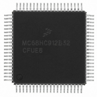
MCHC912B32CFUE8 Freescale Semiconductor, MCHC912B32CFUE8 Datasheet - Page 209

MCHC912B32CFUE8
Manufacturer Part Number
MCHC912B32CFUE8
Description
IC MCU 32K FLASH 8MHZ 80-QFP
Manufacturer
Freescale Semiconductor
Series
HC12r
Datasheet
1.MCHC912B32CFUE8.pdf
(334 pages)
Specifications of MCHC912B32CFUE8
Core Processor
CPU12
Core Size
16-Bit
Speed
8MHz
Connectivity
SCI, SPI
Peripherals
POR, PWM, WDT
Number Of I /o
63
Program Memory Size
32KB (32K x 8)
Program Memory Type
FLASH
Eeprom Size
768 x 8
Ram Size
1K x 8
Voltage - Supply (vcc/vdd)
4.5 V ~ 5.5 V
Data Converters
A/D 8x10b
Oscillator Type
External
Operating Temperature
-40°C ~ 85°C
Package / Case
80-QFP
Cpu Family
HC12
Device Core Size
16b
Frequency (max)
8MHz
Interface Type
SCI/SPI
Total Internal Ram Size
1KB
# I/os (max)
63
Operating Supply Voltage (typ)
5V
Operating Supply Voltage (max)
5.5V
Operating Supply Voltage (min)
4.5V
On-chip Adc
8-chx10-bit
Instruction Set Architecture
CISC
Operating Temp Range
-40C to 85C
Operating Temperature Classification
Industrial
Mounting
Surface Mount
Pin Count
80
Package Type
PQFP
Package
80PQFP
Family Name
HC12
Maximum Speed
8 MHz
Operating Supply Voltage
5 V
Data Bus Width
16 Bit
Number Of Programmable I/os
63
Processor Series
HC912B
Core
HC12
Data Ram Size
1 KB
Maximum Clock Frequency
8 MHz
Maximum Operating Temperature
+ 85 C
Mounting Style
SMD/SMT
3rd Party Development Tools
EWHCS12
Development Tools By Supplier
M68EVB912B32E
Minimum Operating Temperature
- 40 C
Lead Free Status / RoHS Status
Lead free / RoHS Compliant
Available stocks
Company
Part Number
Manufacturer
Quantity
Price
Company:
Part Number:
MCHC912B32CFUE8
Manufacturer:
Freescale Semiconductor
Quantity:
10 000
- Current page: 209 of 334
- Download datasheet (2Mb)
DDS0 — Data Direction for Port S Bit 0
DDS1 — Data Direction for Port S Bit 1
DDS2 and DDS3 — Data Direction for Port S Bit 2 and Bit 3
DDS6–DDS4 — Data Direction for Port S Bits 6–4
DDS7 — Data Direction for Port S Bit 7
14.4.3 Pullup and Reduced Drive Register for Port S
Read: Anytime
Write: Anytime
RDPS2 — Reduce Drive of PS7–PS4
RDPS1 — Reduce Drive of PS3 and PS2
RDPS0 — Reduce Drive of PS1 and PS0
PUPS2 — Pullup Port S Enable PS7–PS4
Freescale Semiconductor
If the SCI receiver is configured for 2-wire SCI operation, corresponding port S pins are input
regardless of the state of these bits.
If the SCI transmitter is configured for 2-wire SCI operation, corresponding port S pins are output
regardless of the state of these bits.
These bits are for general-purpose only.
If the SPI is enabled and expects the corresponding port S pin to be an input, it will be an input
regardless of the state of the DDRS bit. If the SPI is enabled and expects the bit to be an output, it will
be an output only if the DDRS bit is set.
In SPI slave mode, DDS7 has no meaning or effect; the PS7 pin is dedicated as the SS input. In SPI
master mode, DDS7 determines whether PS7 is an error detect input to the SPI or a general-purpose
or slave select output line.
0 = Port S output drivers for bits 7–4 operate normally.
1 = Port S output pins for bits 7–4 have reduced drive capability for lower power and less noise.
0 = Port S output drivers for bits 3 and 2 operate normally.
1 = Port S output pins for bits 3 and 2 have reduced drive capability for lower power and less noise.
0 = Port S output drivers for bits 1 and 0 operate normally.
1 = Port S output pins for bits 1 and 0 have reduced drive capability for lower power and less noise.
0 = No internal pullups on port S bits 7–4.
1 = Port S input pins for bits 7–4 have an active pullup device. If a pin is programmed as output, the
pullup device becomes inactive.
Address:
Reset:
Read:
Figure 14-22. Pullup and Reduced Drive Register for Port S (PURDS)
Write:
$00DB
Bit 7
0
0
= Unimplemented
RDPS2
6
0
M68HC12B Family Data Sheet, Rev. 9.1
RDPS1
5
0
RDPS0
4
0
3
0
0
PUPS2
2
0
PUPS1
1
0
PUPS0
Bit 0
0
Port S
209
Related parts for MCHC912B32CFUE8
Image
Part Number
Description
Manufacturer
Datasheet
Request
R
Part Number:
Description:
Manufacturer:
Freescale Semiconductor, Inc
Datasheet:
Part Number:
Description:
Manufacturer:
Freescale Semiconductor, Inc
Datasheet:
Part Number:
Description:
Manufacturer:
Freescale Semiconductor, Inc
Datasheet:
Part Number:
Description:
Manufacturer:
Freescale Semiconductor, Inc
Datasheet:
Part Number:
Description:
Manufacturer:
Freescale Semiconductor, Inc
Datasheet:
Part Number:
Description:
Manufacturer:
Freescale Semiconductor, Inc
Datasheet:
Part Number:
Description:
Manufacturer:
Freescale Semiconductor, Inc
Datasheet:
Part Number:
Description:
Manufacturer:
Freescale Semiconductor, Inc
Datasheet:
Part Number:
Description:
Manufacturer:
Freescale Semiconductor, Inc
Datasheet:
Part Number:
Description:
Manufacturer:
Freescale Semiconductor, Inc
Datasheet:
Part Number:
Description:
Manufacturer:
Freescale Semiconductor, Inc
Datasheet:
Part Number:
Description:
Manufacturer:
Freescale Semiconductor, Inc
Datasheet:
Part Number:
Description:
Manufacturer:
Freescale Semiconductor, Inc
Datasheet:
Part Number:
Description:
Manufacturer:
Freescale Semiconductor, Inc
Datasheet:
Part Number:
Description:
Manufacturer:
Freescale Semiconductor, Inc
Datasheet:


