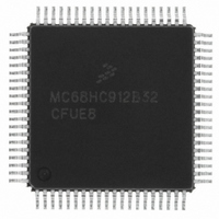
MCHC912B32CFUE8 Freescale Semiconductor, MCHC912B32CFUE8 Datasheet - Page 213

MCHC912B32CFUE8
Manufacturer Part Number
MCHC912B32CFUE8
Description
IC MCU 32K FLASH 8MHZ 80-QFP
Manufacturer
Freescale Semiconductor
Series
HC12r
Datasheet
1.MCHC912B32CFUE8.pdf
(334 pages)
Specifications of MCHC912B32CFUE8
Core Processor
CPU12
Core Size
16-Bit
Speed
8MHz
Connectivity
SCI, SPI
Peripherals
POR, PWM, WDT
Number Of I /o
63
Program Memory Size
32KB (32K x 8)
Program Memory Type
FLASH
Eeprom Size
768 x 8
Ram Size
1K x 8
Voltage - Supply (vcc/vdd)
4.5 V ~ 5.5 V
Data Converters
A/D 8x10b
Oscillator Type
External
Operating Temperature
-40°C ~ 85°C
Package / Case
80-QFP
Cpu Family
HC12
Device Core Size
16b
Frequency (max)
8MHz
Interface Type
SCI/SPI
Total Internal Ram Size
1KB
# I/os (max)
63
Operating Supply Voltage (typ)
5V
Operating Supply Voltage (max)
5.5V
Operating Supply Voltage (min)
4.5V
On-chip Adc
8-chx10-bit
Instruction Set Architecture
CISC
Operating Temp Range
-40C to 85C
Operating Temperature Classification
Industrial
Mounting
Surface Mount
Pin Count
80
Package Type
PQFP
Package
80PQFP
Family Name
HC12
Maximum Speed
8 MHz
Operating Supply Voltage
5 V
Data Bus Width
16 Bit
Number Of Programmable I/os
63
Processor Series
HC912B
Core
HC12
Data Ram Size
1 KB
Maximum Clock Frequency
8 MHz
Maximum Operating Temperature
+ 85 C
Mounting Style
SMD/SMT
3rd Party Development Tools
EWHCS12
Development Tools By Supplier
M68EVB912B32E
Minimum Operating Temperature
- 40 C
Lead Free Status / RoHS Status
Lead free / RoHS Compliant
Available stocks
Company
Part Number
Manufacturer
Quantity
Price
Company:
Part Number:
MCHC912B32CFUE8
Manufacturer:
Freescale Semiconductor
Quantity:
10 000
- Current page: 213 of 334
- Download datasheet (2Mb)
Chapter 15
Byte Data Link Communications (BDLC)
15.1 Introduction
The byte data link communications module (BDLC) provides access to an external serial communication
multiplex bus, operating according to the SAE J1850 protocol.
15.2 Features
Features of the BDLC module include:
15.3 Functional Description
Figure 15-1
addressable registers and provides the link between the CPU and the buffers. The buffers provide storage
for data received and data to be transmitted onto the J1850 bus. The protocol handler is responsible for
the encoding and decoding of data bits and special message symbols during transmission and reception.
The MUX interface provides the link between the BDLC digital section and the analog physical interface.
The wave shaping, driving, and digitizing of data is performed by the physical interface.
Use of the BDLC module in message networking fully implements the SAE Standard J1850 Class B Data
Communication Network Interface specification.
Freescale Semiconductor
•
•
•
•
•
•
•
•
•
•
•
•
SAE J1850 Class B Data Communications Network Interface compatible and ISO compatible for
low-speed (<125 Kbps) serial data communications in automotive applications
10.4 Kbps variable pulse width (VPW) bit format
Digital noise filter
Collision detection
Hardware cyclical redundancy check generation and checking
Two power-saving modes with automatic wakeup on network activity
Polling or CPU interrupts
Block mode receive and transmit
4X receive mode, 41.6 Kbps
Digital loopback mode
Analog loopback mode
In-frame response (IFR) types 0, 1, 2, and 3
shows the organization of the BDLC module. The CPU interface contains the software
Familiarity with the SAE Standard J1850 Class B Data Communication
Network Interface specification is recommended before proceeding.
First-time users of the BDLC should obtain the Byte Data Link Controller
Reference Manual, Freescale document order number BDLCRM/AD.
M68HC12B Family Data Sheet, Rev. 9.1
NOTE
213
Related parts for MCHC912B32CFUE8
Image
Part Number
Description
Manufacturer
Datasheet
Request
R
Part Number:
Description:
Manufacturer:
Freescale Semiconductor, Inc
Datasheet:
Part Number:
Description:
Manufacturer:
Freescale Semiconductor, Inc
Datasheet:
Part Number:
Description:
Manufacturer:
Freescale Semiconductor, Inc
Datasheet:
Part Number:
Description:
Manufacturer:
Freescale Semiconductor, Inc
Datasheet:
Part Number:
Description:
Manufacturer:
Freescale Semiconductor, Inc
Datasheet:
Part Number:
Description:
Manufacturer:
Freescale Semiconductor, Inc
Datasheet:
Part Number:
Description:
Manufacturer:
Freescale Semiconductor, Inc
Datasheet:
Part Number:
Description:
Manufacturer:
Freescale Semiconductor, Inc
Datasheet:
Part Number:
Description:
Manufacturer:
Freescale Semiconductor, Inc
Datasheet:
Part Number:
Description:
Manufacturer:
Freescale Semiconductor, Inc
Datasheet:
Part Number:
Description:
Manufacturer:
Freescale Semiconductor, Inc
Datasheet:
Part Number:
Description:
Manufacturer:
Freescale Semiconductor, Inc
Datasheet:
Part Number:
Description:
Manufacturer:
Freescale Semiconductor, Inc
Datasheet:
Part Number:
Description:
Manufacturer:
Freescale Semiconductor, Inc
Datasheet:
Part Number:
Description:
Manufacturer:
Freescale Semiconductor, Inc
Datasheet:


