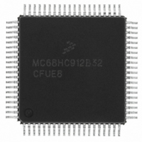
MCHC912B32CFUE8 Freescale Semiconductor, MCHC912B32CFUE8 Datasheet - Page 183

MCHC912B32CFUE8
Manufacturer Part Number
MCHC912B32CFUE8
Description
IC MCU 32K FLASH 8MHZ 80-QFP
Manufacturer
Freescale Semiconductor
Series
HC12r
Datasheet
1.MCHC912B32CFUE8.pdf
(334 pages)
Specifications of MCHC912B32CFUE8
Core Processor
CPU12
Core Size
16-Bit
Speed
8MHz
Connectivity
SCI, SPI
Peripherals
POR, PWM, WDT
Number Of I /o
63
Program Memory Size
32KB (32K x 8)
Program Memory Type
FLASH
Eeprom Size
768 x 8
Ram Size
1K x 8
Voltage - Supply (vcc/vdd)
4.5 V ~ 5.5 V
Data Converters
A/D 8x10b
Oscillator Type
External
Operating Temperature
-40°C ~ 85°C
Package / Case
80-QFP
Cpu Family
HC12
Device Core Size
16b
Frequency (max)
8MHz
Interface Type
SCI/SPI
Total Internal Ram Size
1KB
# I/os (max)
63
Operating Supply Voltage (typ)
5V
Operating Supply Voltage (max)
5.5V
Operating Supply Voltage (min)
4.5V
On-chip Adc
8-chx10-bit
Instruction Set Architecture
CISC
Operating Temp Range
-40C to 85C
Operating Temperature Classification
Industrial
Mounting
Surface Mount
Pin Count
80
Package Type
PQFP
Package
80PQFP
Family Name
HC12
Maximum Speed
8 MHz
Operating Supply Voltage
5 V
Data Bus Width
16 Bit
Number Of Programmable I/os
63
Processor Series
HC912B
Core
HC12
Data Ram Size
1 KB
Maximum Clock Frequency
8 MHz
Maximum Operating Temperature
+ 85 C
Mounting Style
SMD/SMT
3rd Party Development Tools
EWHCS12
Development Tools By Supplier
M68EVB912B32E
Minimum Operating Temperature
- 40 C
Lead Free Status / RoHS Status
Lead free / RoHS Compliant
Available stocks
Company
Part Number
Manufacturer
Quantity
Price
Company:
Part Number:
MCHC912B32CFUE8
Manufacturer:
Freescale Semiconductor
Quantity:
10 000
- Current page: 183 of 334
- Download datasheet (2Mb)
PACMX — 8-Bit Pulse Accumulators Maximum Count Bit
BUFEN — IC Buffer Enable Bit
LATQ — Input Control Latch or Queue Mode Enable Bit
13.4.20 Timer Test Register
Read: Anytime
Write: Only in special mode (SMOD = 1)
Freescale Semiconductor
By setting TFMOD in queue mode, when NOVW bit is set and the corresponding capture and holding
registers are emptied, an input capture event will first update the related input capture register with the
main timer contents. At the next event, the TCn data is transferred to the TCnH register, the TCn is
updated, and the CnF interrupt flag is set. See
interrupt flag is set by a valid external event on PTn.
The BUFEN control bit should be set to enable the IC and pulse accumulators’ holding registers.
Otherwise, LATQ latching modes are disabled.
Writing one into ICLAT bit in MCCTL ($A6), when LATQ and BUFEN are set will produce latching of
input capture and pulse accumulators registers into their holding registers.
0 = The timer flags C3F–C0F in TFLG1 ($8E) are set when a valid input capture transition on the
1 = If in queue mode (BUFEN = 1 and LATQ = 0), the timer flags C3F–C0F in TFLG1 ($8E) are set
0 = Normal operation. When the 8-bit pulse accumulator has reached the value $FF, with the next
1 = When the 8-bit pulse accumulator has reached the value $FF, it will not be incremented further.
0 = Input capture and pulse accumulator holding registers are disabled.
1 = Input capture and pulse accumulator holding registers are enabled. The latching mode is
0 = Queue mode of input capture is enabled. The main timer value is memorized in the IC register
1 = Latch mode is enabled. Latching function occurs when modulus down-counter reaches 0 or a 0
corresponding port pin occurs.
only when a latch on the corresponding holding register occurs. If the queue mode is not
engaged, the timer flags C3F–C0F are set the same way as for TFMOD = 0.
active edge, it will be incremented to $00.
The value $FF indicates a count of 255 or more.
defined by LATQ control bit. Writing a 1 into ICLAT bit in MCCTL ($A6) when LATQ is set, will
produce latching of input capture and pulse accumulator registers into their holding registers.
by a valid input pin transition. With a new occurrence of a capture, the value of the IC register
will be transferred to its holding register and the IC register memorizes the new timer value.
is written into the count register MCCNT (see
event the contents of IC registers and 8-bit pulse accumulators are transferred to their holding
registers. The 8-bit pulse accumulators are cleared.
Address: $00AD
Reset:
Read:
Write:
1. Available only on MC68HC912B32 devices.
Bit 7
0
0
Figure 13-41. Timer Test Register (TIMTST)
= Unimplemented
6
0
0
M68HC12B Family Data Sheet, Rev. 9.1
5
0
0
Figure
4
0
0
13.3.1.2 Buffered IC
13-19. In all other input capture cases, the
3
0
0
2
0
0
TCBYP
Channels). With a latching
1
0
PCBYP
Bit 0
0
(1)
Timer Registers
183
Related parts for MCHC912B32CFUE8
Image
Part Number
Description
Manufacturer
Datasheet
Request
R
Part Number:
Description:
Manufacturer:
Freescale Semiconductor, Inc
Datasheet:
Part Number:
Description:
Manufacturer:
Freescale Semiconductor, Inc
Datasheet:
Part Number:
Description:
Manufacturer:
Freescale Semiconductor, Inc
Datasheet:
Part Number:
Description:
Manufacturer:
Freescale Semiconductor, Inc
Datasheet:
Part Number:
Description:
Manufacturer:
Freescale Semiconductor, Inc
Datasheet:
Part Number:
Description:
Manufacturer:
Freescale Semiconductor, Inc
Datasheet:
Part Number:
Description:
Manufacturer:
Freescale Semiconductor, Inc
Datasheet:
Part Number:
Description:
Manufacturer:
Freescale Semiconductor, Inc
Datasheet:
Part Number:
Description:
Manufacturer:
Freescale Semiconductor, Inc
Datasheet:
Part Number:
Description:
Manufacturer:
Freescale Semiconductor, Inc
Datasheet:
Part Number:
Description:
Manufacturer:
Freescale Semiconductor, Inc
Datasheet:
Part Number:
Description:
Manufacturer:
Freescale Semiconductor, Inc
Datasheet:
Part Number:
Description:
Manufacturer:
Freescale Semiconductor, Inc
Datasheet:
Part Number:
Description:
Manufacturer:
Freescale Semiconductor, Inc
Datasheet:
Part Number:
Description:
Manufacturer:
Freescale Semiconductor, Inc
Datasheet:


