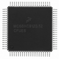
MCHC912B32CFUE8 Freescale Semiconductor, MCHC912B32CFUE8 Datasheet - Page 294

MCHC912B32CFUE8
Manufacturer Part Number
MCHC912B32CFUE8
Description
IC MCU 32K FLASH 8MHZ 80-QFP
Manufacturer
Freescale Semiconductor
Series
HC12r
Datasheet
1.MCHC912B32CFUE8.pdf
(334 pages)
Specifications of MCHC912B32CFUE8
Core Processor
CPU12
Core Size
16-Bit
Speed
8MHz
Connectivity
SCI, SPI
Peripherals
POR, PWM, WDT
Number Of I /o
63
Program Memory Size
32KB (32K x 8)
Program Memory Type
FLASH
Eeprom Size
768 x 8
Ram Size
1K x 8
Voltage - Supply (vcc/vdd)
4.5 V ~ 5.5 V
Data Converters
A/D 8x10b
Oscillator Type
External
Operating Temperature
-40°C ~ 85°C
Package / Case
80-QFP
Cpu Family
HC12
Device Core Size
16b
Frequency (max)
8MHz
Interface Type
SCI/SPI
Total Internal Ram Size
1KB
# I/os (max)
63
Operating Supply Voltage (typ)
5V
Operating Supply Voltage (max)
5.5V
Operating Supply Voltage (min)
4.5V
On-chip Adc
8-chx10-bit
Instruction Set Architecture
CISC
Operating Temp Range
-40C to 85C
Operating Temperature Classification
Industrial
Mounting
Surface Mount
Pin Count
80
Package Type
PQFP
Package
80PQFP
Family Name
HC12
Maximum Speed
8 MHz
Operating Supply Voltage
5 V
Data Bus Width
16 Bit
Number Of Programmable I/os
63
Processor Series
HC912B
Core
HC12
Data Ram Size
1 KB
Maximum Clock Frequency
8 MHz
Maximum Operating Temperature
+ 85 C
Mounting Style
SMD/SMT
3rd Party Development Tools
EWHCS12
Development Tools By Supplier
M68EVB912B32E
Minimum Operating Temperature
- 40 C
Lead Free Status / RoHS Status
Lead free / RoHS Compliant
Available stocks
Company
Part Number
Manufacturer
Quantity
Price
Company:
Part Number:
MCHC912B32CFUE8
Manufacturer:
Freescale Semiconductor
Quantity:
10 000
- Current page: 294 of 334
- Download datasheet (2Mb)
Development Support
The second type of BDM commands are called firmware commands because they are implemented in a
small ROM within the HC12 MCU. The CPU must be in background mode to execute firmware
commands. The usual way to get to background mode is by the hardware command BACKGROUND. The
BDM ROM is located at $FF20 to $FFFF while BDM is active. There are also seven bytes of BDM
registers which are located at $FF00 to $FF06 while BDM is active. The CPU executes code from this
ROM to perform the requested operation. The BDM firmware watches for serial commands and executes
them as they are received. The firmware commands are shown in
Each of the hardware and firmware BDM commands starts with an 8-bit command code (opcode).
Depending upon the commands, a 16-bit address and/or a 16-bit data word is required as indicated in the
tables by the command. All the read commands output 16 bits of data despite the byte/word implication
in the command name.
294
1. STATUS command is a specific case of the READ_BD_BYTE command.
2. ENABLE_FIRMWARE is a specific case of the WRITE_BD_BYTE command.
WRITE_BD_WORD
WRITE_WORD
WRITE_BYTE
Command
WRITE_NEXT
READ_NEXT
WRITE_PC
WRITE_SP
Command
READ_PC
READ_SP
WRITE_D
WRITE_X
WRITE_Y
READ_D
READ_X
READ_Y
TRACE1
TAGGO
GO
Opcode (Hex)
Table 18-2. BDM Hardware Commands (Continued)
CC
C0
C8
Opcode (Hex)
Table 18-3. BDM Firmware Commands
M68HC12B Family Data Sheet, Rev. 9.1
62
63
64
65
66
67
42
43
44
45
46
47
08
10
18
16-bit address
16-bit address
16-bit address
16-bit data in
16-bit data in
16-bit data in
Data
16-bit data out
16-bit data out
16-bit data out
16-bit data out
16-bit data out
16-bit data out
16-bit data in
16-bit data in
16-bit data in
16-bit data in
16-bit data in
16-bit data in
None
None
None
Data
Write to memory with BDM in map (may steal cycles if external
access) must be aligned access.
Write to memory with BDM out of map (may steal cycles if
external access) data for odd address on low byte, data for even
address on high byte.
Write to memory with BDM out of map (may steal cycles if
external access) must be aligned access.
X = X + 2; Read next word
pointed to by X
Read program counter
Read D accumulator
Read X index register
Read Y index register
Read stack pointer
X = X + 2; Write next word
pointed to by X
Write program counter
Write D accumulator
Write X index register
Write Y index register
Write stack pointer
Go to user program
Execute one user instruction
then return to BDM
Enable tagging and go to
user program
Table
Description
Description
18-3.
Freescale Semiconductor
Related parts for MCHC912B32CFUE8
Image
Part Number
Description
Manufacturer
Datasheet
Request
R
Part Number:
Description:
Manufacturer:
Freescale Semiconductor, Inc
Datasheet:
Part Number:
Description:
Manufacturer:
Freescale Semiconductor, Inc
Datasheet:
Part Number:
Description:
Manufacturer:
Freescale Semiconductor, Inc
Datasheet:
Part Number:
Description:
Manufacturer:
Freescale Semiconductor, Inc
Datasheet:
Part Number:
Description:
Manufacturer:
Freescale Semiconductor, Inc
Datasheet:
Part Number:
Description:
Manufacturer:
Freescale Semiconductor, Inc
Datasheet:
Part Number:
Description:
Manufacturer:
Freescale Semiconductor, Inc
Datasheet:
Part Number:
Description:
Manufacturer:
Freescale Semiconductor, Inc
Datasheet:
Part Number:
Description:
Manufacturer:
Freescale Semiconductor, Inc
Datasheet:
Part Number:
Description:
Manufacturer:
Freescale Semiconductor, Inc
Datasheet:
Part Number:
Description:
Manufacturer:
Freescale Semiconductor, Inc
Datasheet:
Part Number:
Description:
Manufacturer:
Freescale Semiconductor, Inc
Datasheet:
Part Number:
Description:
Manufacturer:
Freescale Semiconductor, Inc
Datasheet:
Part Number:
Description:
Manufacturer:
Freescale Semiconductor, Inc
Datasheet:
Part Number:
Description:
Manufacturer:
Freescale Semiconductor, Inc
Datasheet:


