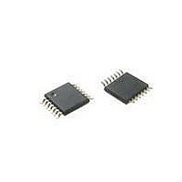
ATTINY20-XU Atmel, ATTINY20-XU Datasheet - Page 82

ATTINY20-XU
Manufacturer Part Number
ATTINY20-XU
Description
MCU AVR 2KB FLASH 12MHZ 14TSSOP
Manufacturer
Atmel
Series
AVR® ATtinyr
Datasheet
1.ATTINY20-EK1.pdf
(224 pages)
Specifications of ATTINY20-XU
Core Processor
AVR
Core Size
8-Bit
Speed
12MHz
Connectivity
I²C, SPI
Peripherals
Brown-out Detect/Reset, POR, PWM, WDT
Number Of I /o
12
Program Memory Size
2KB (1K x 16)
Program Memory Type
FLASH
Ram Size
128 x 8
Voltage - Supply (vcc/vdd)
1.8 V ~ 5.5 V
Data Converters
A/D 8x10b
Oscillator Type
Internal
Operating Temperature
-40°C ~ 85°C
Package / Case
*
Processor Series
ATtiny
Core
AVR
Data Bus Width
8 bit
Data Ram Size
128 B
Interface Type
SPI, TWI
Maximum Clock Frequency
12 MHz
Number Of Programmable I/os
12
Number Of Timers
2
Operating Supply Voltage
3.3 V
Maximum Operating Temperature
+ 85 C
Mounting Style
SMD/SMT
Minimum Operating Temperature
- 40 C
Operating Temperature Range
- 40 C to + 85 C
Lead Free Status / RoHS Status
Lead free / RoHS Compliant
Eeprom Size
-
Lead Free Status / Rohs Status
Details
Available stocks
Company
Part Number
Manufacturer
Quantity
Price
Company:
Part Number:
ATTINY20-XU
Manufacturer:
Atmel
Quantity:
904
- Current page: 82 of 224
- Download datasheet (6Mb)
12.5.1
12.5.2
12.5.3
82
ATtiny20
Input Capture Trigger Source
Noise Canceler
Using the Input Capture Unit
cleared when the interrupt is executed. Alternatively the ICF1 flag can be cleared by software by
writing a logical one to its I/O bit location.
Reading the 16-bit value in the Input Capture Register (ICR1) is done by first reading the low
byte (ICR1L) and then the high byte (ICR1H). When the low byte is read the high byte is copied
into the high byte temporary register (TEMP). When the CPU reads the ICR1H I/O location it will
access the TEMP Register.
The ICR1 Register can only be written when using a Waveform Generation mode that utilizes
the ICR1 Register for defining the counter’s TOP value. In these cases the Waveform Genera-
tion mode (WGM1[3:0]) bits must be set before the TOP value can be written to the ICR1
Register. When writing the ICR1 Register the high byte must be written to the ICR1H I/O location
before the low byte is written to ICR1L.
For more information on how to access the 16-bit registers refer to
on page
The main trigger source for the Input Capture unit is the Input Capture pin (ICP1).
Timer/Counter1 can alternatively use the Analog Comparator output as trigger source for the
Input Capture unit. The Analog Comparator is selected as trigger source by setting the Analog
Comparator Input Capture (ACIC) bit in the Analog Comparator Control and Status Register
(ACSR). Be aware that changing trigger source can trigger a capture. The Input Capture Flag
must therefore be cleared after the change.
Both the Input Capture pin (ICP1) and the Analog Comparator output (ACO) inputs are sampled
using the same technique as for the T1 pin
identical. However, when the noise canceler is enabled, additional logic is inserted before the
edge detector, which increases the delay by four system clock cycles. Note that the input of the
noise canceler and edge detector is always enabled unless the Timer/Counter is set in a Wave-
form Generation mode that uses ICR1 to define TOP.
An Input Capture can be triggered by software by controlling the port of the ICP1 pin.
The noise canceler uses a simple digital filtering technique to improve noise immunity. Consecu-
tive samples are monitored in a pipeline four units deep. The signal going to the edge detecter is
allowed to change only when all four samples are equal.
The noise canceler is enabled by setting the Input Capture Noise Canceler (ICNC1) bit in
Timer/Counter Control Register B (TCCR1B). When enabled, the noise canceler introduces an
additional delay of four system clock cycles to a change applied to the input and before ICR1 is
updated.
The noise canceler uses the system clock directly and is therefore not affected by the prescaler.
The main challenge when using the Input Capture unit is to assign enough processor capacity
for handling the incoming events. The time between two events is critical. If the processor has
not read the captured value in the ICR1 Register before the next event occurs, the ICR1 will be
overwritten with a new value. In this case the result of the capture will be incorrect.
When using the Input Capture interrupt, the ICR1 Register should be read as early in the inter-
rupt handler routine as possible. Even though the Input Capture interrupt has relatively high
95.
(Figure 13-1 on page
105). The edge detector is also
“Accessing 16-bit Registers”
8235B–AVR–04/11
Related parts for ATTINY20-XU
Image
Part Number
Description
Manufacturer
Datasheet
Request
R

Part Number:
Description:
IC, MCU, 8BIT, 2K FLASH, 20SOIC
Manufacturer:
Atmel
Datasheet:

Part Number:
Description:
IC, MCU, 8BIT, 2K FLASH, 20PDIP
Manufacturer:
Atmel
Datasheet:

Part Number:
Description:
IC, MCU, 8BIT, 8K FLASH, 20PDIP
Manufacturer:
Atmel
Datasheet:

Part Number:
Description:
IC, MCU, 8BIT, 8K FLASH, 20SOIC
Manufacturer:
Atmel
Datasheet:

Part Number:
Description:
DEV KIT FOR AVR/AVR32
Manufacturer:
Atmel
Datasheet:

Part Number:
Description:
INTERVAL AND WIPE/WASH WIPER CONTROL IC WITH DELAY
Manufacturer:
ATMEL Corporation
Datasheet:

Part Number:
Description:
Low-Voltage Voice-Switched IC for Hands-Free Operation
Manufacturer:
ATMEL Corporation
Datasheet:

Part Number:
Description:
MONOLITHIC INTEGRATED FEATUREPHONE CIRCUIT
Manufacturer:
ATMEL Corporation
Datasheet:

Part Number:
Description:
AM-FM Receiver IC U4255BM-M
Manufacturer:
ATMEL Corporation
Datasheet:

Part Number:
Description:
Monolithic Integrated Feature Phone Circuit
Manufacturer:
ATMEL Corporation
Datasheet:

Part Number:
Description:
Multistandard Video-IF and Quasi Parallel Sound Processing
Manufacturer:
ATMEL Corporation
Datasheet:

Part Number:
Description:
High-performance EE PLD
Manufacturer:
ATMEL Corporation
Datasheet:


