ATTINY20-XU Atmel, ATTINY20-XU Datasheet - Page 167
ATTINY20-XU
Manufacturer Part Number
ATTINY20-XU
Description
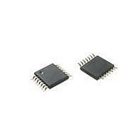
MCU AVR 2KB FLASH 12MHZ 14TSSOP
Manufacturer
Atmel
Series
AVR® ATtinyr
Datasheet
1.ATTINY20-EK1.pdf
(224 pages)
Specifications of ATTINY20-XU
Core Processor
AVR
Core Size
8-Bit
Speed
12MHz
Connectivity
I²C, SPI
Peripherals
Brown-out Detect/Reset, POR, PWM, WDT
Number Of I /o
12
Program Memory Size
2KB (1K x 16)
Program Memory Type
FLASH
Ram Size
128 x 8
Voltage - Supply (vcc/vdd)
1.8 V ~ 5.5 V
Data Converters
A/D 8x10b
Oscillator Type
Internal
Operating Temperature
-40°C ~ 85°C
Package / Case
*
Processor Series
ATtiny
Core
AVR
Data Bus Width
8 bit
Data Ram Size
128 B
Interface Type
SPI, TWI
Maximum Clock Frequency
12 MHz
Number Of Programmable I/os
12
Number Of Timers
2
Operating Supply Voltage
3.3 V
Maximum Operating Temperature
+ 85 C
Mounting Style
SMD/SMT
Minimum Operating Temperature
- 40 C
Operating Temperature Range
- 40 C to + 85 C
Lead Free Status / RoHS Status
Lead free / RoHS Compliant
Eeprom Size
-
Lead Free Status / Rohs Status
Details
Available stocks
Company
Part Number
Manufacturer
Quantity
Price
Company:

Part Number:
ATTINY20-XU
Manufacturer:
Atmel
Quantity:
904


19.4
19.4.1
8235B–AVR–04/11
Accessing the NVM
Addressing the Flash
NVM lock bits, and all Flash memory sections are mapped to the data space as shown in
5-1 on page
in the data space.
The NVM Controller recognises a set of commands that can be used to instruct the controller
what type of programming task to perform on the NVM. Commands to the NVM Controller are
issued via the NVM Command Register. See
Register” on page
writing data to the NVM locations mapped to the data space.
When the NVM Controller is busy performing an operation it will signal this via the NVM Busy
Flag in the NVM Control and Status Register. See
Status Register” on page
as the busy flag is active. This is to ensure that the current command is fully executed before a
new command can start.
Programming any part of the NVM will automatically inhibit the following operations:
The ATtiny20 supports only external programming. Internal programming operations to the NVM
have been disabled, which means any internal attempt to write or erase NVM locations will fail.
The data space uses byte accessing but since the Flash sections are accessed as words and
organized in pages, the byte-address of the data space must be converted to the word-address
of the Flash section. This is illustrated in
Figure 19-1. Addressing the Flash Memory
• All programming to any other part of the NVM
• All reading from any NVM location
ADDRESS POINTER
SECTIONEND
16
16. The NVM can be accessed for read and programming via the locations mapped
00
01
02
...
...
...
SECTION
FLASH
170. After the selected command has been loaded, the operation is started by
PAGE
171. The NVM Command Register is blocked for write access as long
PADDRMSB
WITHIN A FLASH
PAGE ADDRESS
Figure
SECTION
PADDR
PAGEEND
19-1. Also, see
“NVMCMD – Non-Volatile Memory Command
“NVMCSR - Non-Volatile Memory Control and
00
01
...
...
...
WADDRMSB+1
FLASH
WORD
PAGE
Table 19-3 on page
WADDRMSB
WADDR
WORD ADDRESS
WITHIN A FLASH
PAGE
1
ATtiny20
0/1
LOW/HIGH
BYTE SELECT
165.
Figure
167
Related parts for ATTINY20-XU
Image
Part Number
Description
Manufacturer
Datasheet
Request
R

Part Number:
Description:
IC, MCU, 8BIT, 2K FLASH, 20SOIC
Manufacturer:
Atmel
Datasheet:

Part Number:
Description:
IC, MCU, 8BIT, 2K FLASH, 20PDIP
Manufacturer:
Atmel
Datasheet:
Part Number:
Description:
IC, MCU, 8BIT, 8K FLASH, 20PDIP
Manufacturer:
Atmel
Datasheet:
Part Number:
Description:
IC, MCU, 8BIT, 8K FLASH, 20SOIC
Manufacturer:
Atmel
Datasheet:

Part Number:
Description:
DEV KIT FOR AVR/AVR32
Manufacturer:
Atmel
Datasheet:

Part Number:
Description:
INTERVAL AND WIPE/WASH WIPER CONTROL IC WITH DELAY
Manufacturer:
ATMEL Corporation
Datasheet:
Part Number:
Description:
Low-Voltage Voice-Switched IC for Hands-Free Operation
Manufacturer:
ATMEL Corporation
Datasheet:
Part Number:
Description:
MONOLITHIC INTEGRATED FEATUREPHONE CIRCUIT
Manufacturer:
ATMEL Corporation
Datasheet:
Part Number:
Description:
AM-FM Receiver IC U4255BM-M
Manufacturer:
ATMEL Corporation
Datasheet:
Part Number:
Description:
Monolithic Integrated Feature Phone Circuit
Manufacturer:
ATMEL Corporation
Datasheet:
Part Number:
Description:
Multistandard Video-IF and Quasi Parallel Sound Processing
Manufacturer:
ATMEL Corporation
Datasheet:
Part Number:
Description:
High-performance EE PLD
Manufacturer:
ATMEL Corporation
Datasheet: