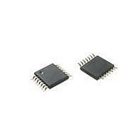
ATTINY20-XU Atmel, ATTINY20-XU Datasheet - Page 52

ATTINY20-XU
Manufacturer Part Number
ATTINY20-XU
Description
MCU AVR 2KB FLASH 12MHZ 14TSSOP
Manufacturer
Atmel
Series
AVR® ATtinyr
Datasheet
1.ATTINY20-EK1.pdf
(224 pages)
Specifications of ATTINY20-XU
Core Processor
AVR
Core Size
8-Bit
Speed
12MHz
Connectivity
I²C, SPI
Peripherals
Brown-out Detect/Reset, POR, PWM, WDT
Number Of I /o
12
Program Memory Size
2KB (1K x 16)
Program Memory Type
FLASH
Ram Size
128 x 8
Voltage - Supply (vcc/vdd)
1.8 V ~ 5.5 V
Data Converters
A/D 8x10b
Oscillator Type
Internal
Operating Temperature
-40°C ~ 85°C
Package / Case
*
Processor Series
ATtiny
Core
AVR
Data Bus Width
8 bit
Data Ram Size
128 B
Interface Type
SPI, TWI
Maximum Clock Frequency
12 MHz
Number Of Programmable I/os
12
Number Of Timers
2
Operating Supply Voltage
3.3 V
Maximum Operating Temperature
+ 85 C
Mounting Style
SMD/SMT
Minimum Operating Temperature
- 40 C
Operating Temperature Range
- 40 C to + 85 C
Lead Free Status / RoHS Status
Lead free / RoHS Compliant
Eeprom Size
-
Lead Free Status / Rohs Status
Details
Available stocks
Company
Part Number
Manufacturer
Quantity
Price
Company:
Part Number:
ATTINY20-XU
Manufacturer:
Atmel
Quantity:
904
- Current page: 52 of 224
- Download datasheet (6Mb)
10.3.1
52
ATtiny20
Alternate Functions of Port A
The Port A pins with alternate function are shown in
Table 10-3.
• Port A, Bit 0 – ADC0/PCINT0
• Port A, Bit 1 – ADC1/AIN0/PCINT1
• ADC0: Analog to Digital Converter, Channel 0
• PCINT0: Pin Change Interrupt source 0. The PA0 pin can serve as an external interrupt
• ADC1: Analog to Digital Converter, Channel 1
• AIN0: Analog Comparator Positive Input. Configure the port pin as input with the internal pull-
• PCINT1: Pin Change Interrupt source 1. The PA1 pin can serve as an external interrupt
source for pin change interrupt 0.
up switched off to avoid the digital port function from interfering with the function of the
Analog Comparator.
source for pin change interrupt 0.
Port Pin
PA0
PA1
PA2
PA3
PA4
PA5
PA6
PA7
Port A Pins Alternate Functions
Alternate Function
ADC0:
PCINT0: Pin Change Interrupt 0, Source 0
ADC1:
AIN0:
PCINT1:Pin Change Interrupt 0, Source 1
ADC2:
AIN1:
PCINT2: Pin Change Interrupt 0, Source 2
ADC3:
PCINT3: Pin Change Interrupt 0, Source 3
ADC4:
PCINT4: Pin Change Interrupt 0, Source 4
ADC5:
PCINT5: Pin Change Interrupt 0, Source 5
ADC6:
SS :
PCINT6: Pin Change Interrupt 0, Source 6
ADC7:
OC0B:: Timer/Counter0 Compare Match B Output
ICP1:
T1:
SCL:
SCK:
PCINT7: Pin Change Interrupt 0, Source 7
ADC Input Channel 0
ADC Input Channel 1
Analog Comparator, Positive Input
ADC Input Channel 2
Analog Comparator, Negative Input
ADC Input Channel 3
ADC Input Channel 4
ADC Input Channel 5
ADC Input Channel 6
SPI Slave Select
ADC Input Channel 7
Timer/Counter1 Input Capture Pin
Timer/Counter1 Clock Source
TWI Clock
SPI Clock
.
.
Table
10-3.
8235B–AVR–04/11
Related parts for ATTINY20-XU
Image
Part Number
Description
Manufacturer
Datasheet
Request
R

Part Number:
Description:
IC, MCU, 8BIT, 2K FLASH, 20SOIC
Manufacturer:
Atmel
Datasheet:

Part Number:
Description:
IC, MCU, 8BIT, 2K FLASH, 20PDIP
Manufacturer:
Atmel
Datasheet:

Part Number:
Description:
IC, MCU, 8BIT, 8K FLASH, 20PDIP
Manufacturer:
Atmel
Datasheet:

Part Number:
Description:
IC, MCU, 8BIT, 8K FLASH, 20SOIC
Manufacturer:
Atmel
Datasheet:

Part Number:
Description:
DEV KIT FOR AVR/AVR32
Manufacturer:
Atmel
Datasheet:

Part Number:
Description:
INTERVAL AND WIPE/WASH WIPER CONTROL IC WITH DELAY
Manufacturer:
ATMEL Corporation
Datasheet:

Part Number:
Description:
Low-Voltage Voice-Switched IC for Hands-Free Operation
Manufacturer:
ATMEL Corporation
Datasheet:

Part Number:
Description:
MONOLITHIC INTEGRATED FEATUREPHONE CIRCUIT
Manufacturer:
ATMEL Corporation
Datasheet:

Part Number:
Description:
AM-FM Receiver IC U4255BM-M
Manufacturer:
ATMEL Corporation
Datasheet:

Part Number:
Description:
Monolithic Integrated Feature Phone Circuit
Manufacturer:
ATMEL Corporation
Datasheet:

Part Number:
Description:
Multistandard Video-IF and Quasi Parallel Sound Processing
Manufacturer:
ATMEL Corporation
Datasheet:

Part Number:
Description:
High-performance EE PLD
Manufacturer:
ATMEL Corporation
Datasheet:


