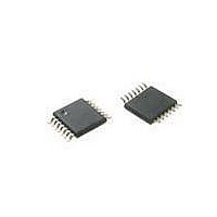
ATTINY20-XU Atmel, ATTINY20-XU Datasheet - Page 168

ATTINY20-XU
Manufacturer Part Number
ATTINY20-XU
Description
MCU AVR 2KB FLASH 12MHZ 14TSSOP
Manufacturer
Atmel
Series
AVR® ATtinyr
Datasheet
1.ATTINY20-EK1.pdf
(224 pages)
Specifications of ATTINY20-XU
Core Processor
AVR
Core Size
8-Bit
Speed
12MHz
Connectivity
I²C, SPI
Peripherals
Brown-out Detect/Reset, POR, PWM, WDT
Number Of I /o
12
Program Memory Size
2KB (1K x 16)
Program Memory Type
FLASH
Ram Size
128 x 8
Voltage - Supply (vcc/vdd)
1.8 V ~ 5.5 V
Data Converters
A/D 8x10b
Oscillator Type
Internal
Operating Temperature
-40°C ~ 85°C
Package / Case
*
Processor Series
ATtiny
Core
AVR
Data Bus Width
8 bit
Data Ram Size
128 B
Interface Type
SPI, TWI
Maximum Clock Frequency
12 MHz
Number Of Programmable I/os
12
Number Of Timers
2
Operating Supply Voltage
3.3 V
Maximum Operating Temperature
+ 85 C
Mounting Style
SMD/SMT
Minimum Operating Temperature
- 40 C
Operating Temperature Range
- 40 C to + 85 C
Lead Free Status / RoHS Status
Lead free / RoHS Compliant
Eeprom Size
-
Lead Free Status / Rohs Status
Details
Available stocks
Company
Part Number
Manufacturer
Quantity
Price
Company:
Part Number:
ATTINY20-XU
Manufacturer:
Atmel
Quantity:
904
- Current page: 168 of 224
- Download datasheet (6Mb)
19.4.2
19.4.3
19.4.3.1
168
ATtiny20
Reading the Flash
Programming the Flash
Chip Erase
The most significant bits of the data space address select the NVM Lock bits or the Flash sec-
tion mapped to the data memory. The word address within a page (WADDR) is held by the bits
[WADDRMSB:1], and the page address (PADDR) is held by the bits [PADDRMSB:WAD-
DRMSB+1]. Together, PADDR and WADDR form the absolute address of a word in the Flash
section.
The least significant bit of the Flash section address is used to select the low or high byte of the
word.
The Flash can be read from the data memory mapped locations one byte at a time. For read
operations, the least significant bit (bit 0) is used to select the low or high byte in the word
address. If this bit is zero, the low byte is read, and if it is one, the high byte is read.
The Flash can be written two words at a time. Before writing a Flash double word, the Flash tar-
get location must be erased. Writing to an un-erased Flash word will corrupt its content.
The Flash is written two words at a time but the data space uses byte-addressing to access
Flash that has been mapped to data memory. It is therefore important to write the two words in
the correct order to the Flash, namely low bytes before high bytes. The low byte of the first word
is first written to the temporary buffer, then the high byte. Writing the low byte and then the high
byte to the buffer latches the two words into the Flash write buffer, starting the actual Flash write
operation.
The Flash erase operations can only performed for the entire Flash sections.
The Flash programming sequence is as follows:
The Chip Erase command will erase the entire code section of the Flash memory and the NVM
Lock Bits. For security reasons, however, the NVM Lock Bits are not reset before the code sec-
tion has been completely erased. The Configuration, Signature and Calibration sections are not
changed.
Before starting the Chip erase, the NVMCMD register must be loaded with the CHIP_ERASE
command. To start the erase operation a dummy byte must be written into the high byte of a
word location that resides inside the Flash code section. The NVMBSY bit remains set until eras-
ing has been completed. While the Flash is being erased neither Flash buffer loading nor Flash
reading can be performed.
The Chip Erase can be carried out as follows:
1. Perform a Flash section erase or perform a Chip erase
2. Write the Flash section two words at a time
1. Write the CHIP_ERASE command to the NVMCMD register
2. Start the erase operation by writing a dummy byte to the high byte of any word location
3. Wait until the NVMBSY bit has been cleared
inside the code section
8235B–AVR–04/11
Related parts for ATTINY20-XU
Image
Part Number
Description
Manufacturer
Datasheet
Request
R

Part Number:
Description:
IC, MCU, 8BIT, 2K FLASH, 20SOIC
Manufacturer:
Atmel
Datasheet:

Part Number:
Description:
IC, MCU, 8BIT, 2K FLASH, 20PDIP
Manufacturer:
Atmel
Datasheet:

Part Number:
Description:
IC, MCU, 8BIT, 8K FLASH, 20PDIP
Manufacturer:
Atmel
Datasheet:

Part Number:
Description:
IC, MCU, 8BIT, 8K FLASH, 20SOIC
Manufacturer:
Atmel
Datasheet:

Part Number:
Description:
DEV KIT FOR AVR/AVR32
Manufacturer:
Atmel
Datasheet:

Part Number:
Description:
INTERVAL AND WIPE/WASH WIPER CONTROL IC WITH DELAY
Manufacturer:
ATMEL Corporation
Datasheet:

Part Number:
Description:
Low-Voltage Voice-Switched IC for Hands-Free Operation
Manufacturer:
ATMEL Corporation
Datasheet:

Part Number:
Description:
MONOLITHIC INTEGRATED FEATUREPHONE CIRCUIT
Manufacturer:
ATMEL Corporation
Datasheet:

Part Number:
Description:
AM-FM Receiver IC U4255BM-M
Manufacturer:
ATMEL Corporation
Datasheet:

Part Number:
Description:
Monolithic Integrated Feature Phone Circuit
Manufacturer:
ATMEL Corporation
Datasheet:

Part Number:
Description:
Multistandard Video-IF and Quasi Parallel Sound Processing
Manufacturer:
ATMEL Corporation
Datasheet:

Part Number:
Description:
High-performance EE PLD
Manufacturer:
ATMEL Corporation
Datasheet:


