ATTINY20-XU Atmel, ATTINY20-XU Datasheet - Page 47
ATTINY20-XU
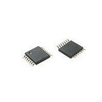
Manufacturer Part Number
ATTINY20-XU
Description
MCU AVR 2KB FLASH 12MHZ 14TSSOP
Manufacturer
Atmel
Series
AVR® ATtinyr
Datasheet
1.ATTINY20-EK1.pdf
(224 pages)
Specifications of ATTINY20-XU
Core Processor
AVR
Core Size
8-Bit
Speed
12MHz
Connectivity
I²C, SPI
Peripherals
Brown-out Detect/Reset, POR, PWM, WDT
Number Of I /o
12
Program Memory Size
2KB (1K x 16)
Program Memory Type
FLASH
Ram Size
128 x 8
Voltage - Supply (vcc/vdd)
1.8 V ~ 5.5 V
Data Converters
A/D 8x10b
Oscillator Type
Internal
Operating Temperature
-40°C ~ 85°C
Package / Case
*
Processor Series
ATtiny
Core
AVR
Data Bus Width
8 bit
Data Ram Size
128 B
Interface Type
SPI, TWI
Maximum Clock Frequency
12 MHz
Number Of Programmable I/os
12
Number Of Timers
2
Operating Supply Voltage
3.3 V
Maximum Operating Temperature
+ 85 C
Mounting Style
SMD/SMT
Minimum Operating Temperature
- 40 C
Operating Temperature Range
- 40 C to + 85 C
Lead Free Status / RoHS Status
Lead free / RoHS Compliant
Eeprom Size
-
Lead Free Status / Rohs Status
Details
Available stocks
Company
Part Number
Manufacturer
Quantity
Price
Company:

Part Number:
ATTINY20-XU
Manufacturer:
Atmel
Quantity:
904


10.2.4
8235B–AVR–04/11
Reading the Pin Value
Figure 10-3. Switching Between Input and Output in Break-Before-Make-Mode
Independent of the setting of Data Direction bit DDxn, the port pin can be read through the
PINxn Register bit. As shown in
ing latch constitute a synchronizer. This is needed to avoid metastability if the physical pin
changes value near the edge of the internal clock, but it also introduces a delay.
shows a timing diagram of the synchronization when reading an externally applied pin value.
The maximum and minimum propagation delays are denoted t
Figure 10-4. Synchronization when Reading an Externally Applied Pin value
Consider the clock period starting shortly after the first falling edge of the system clock. The latch
is closed when the clock is low, and goes transparent when the clock is high, as indicated by the
shaded region of the “SYNC LATCH” signal. The signal value is latched when the system clock
goes low. It is clocked into the PINxn Register at the succeeding positive clock edge. As indi-
cated by the two arrows tpd,max and tpd,min, a single signal transition on the pin will be delayed
between ½ and 1½ system clock period depending upon the time of assertion.
INSTRUCTIONS
SYSTEM CLK
INSTRUCTIONS
SYSTEM CLK
SYNC LATCH
PORTx
DDRx
Px0
Px1
r16
r17
PINxn
r17
0x01
tri-state
out DDRx, r16
Figure 10-2 on page
XXX
intermediate tri-state cycle
0x02
tri-state
nop
t
pd, max
0x02
0x01
0x55
0x00
XXX
45, the PINxn Register bit and the preced-
out DDRx, r17
t
pd, min
pd,max
in r17, PINx
and t
intermediate tri-state cycle
tri-state
0x01
pd,min
respectively.
ATtiny20
0xFF
Figure 10-4
47
Related parts for ATTINY20-XU
Image
Part Number
Description
Manufacturer
Datasheet
Request
R

Part Number:
Description:
IC, MCU, 8BIT, 2K FLASH, 20SOIC
Manufacturer:
Atmel
Datasheet:

Part Number:
Description:
IC, MCU, 8BIT, 2K FLASH, 20PDIP
Manufacturer:
Atmel
Datasheet:
Part Number:
Description:
IC, MCU, 8BIT, 8K FLASH, 20PDIP
Manufacturer:
Atmel
Datasheet:
Part Number:
Description:
IC, MCU, 8BIT, 8K FLASH, 20SOIC
Manufacturer:
Atmel
Datasheet:

Part Number:
Description:
DEV KIT FOR AVR/AVR32
Manufacturer:
Atmel
Datasheet:

Part Number:
Description:
INTERVAL AND WIPE/WASH WIPER CONTROL IC WITH DELAY
Manufacturer:
ATMEL Corporation
Datasheet:
Part Number:
Description:
Low-Voltage Voice-Switched IC for Hands-Free Operation
Manufacturer:
ATMEL Corporation
Datasheet:
Part Number:
Description:
MONOLITHIC INTEGRATED FEATUREPHONE CIRCUIT
Manufacturer:
ATMEL Corporation
Datasheet:
Part Number:
Description:
AM-FM Receiver IC U4255BM-M
Manufacturer:
ATMEL Corporation
Datasheet:
Part Number:
Description:
Monolithic Integrated Feature Phone Circuit
Manufacturer:
ATMEL Corporation
Datasheet:
Part Number:
Description:
Multistandard Video-IF and Quasi Parallel Sound Processing
Manufacturer:
ATMEL Corporation
Datasheet:
Part Number:
Description:
High-performance EE PLD
Manufacturer:
ATMEL Corporation
Datasheet: