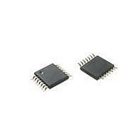
ATTINY20-XU Atmel, ATTINY20-XU Datasheet - Page 123

ATTINY20-XU
Manufacturer Part Number
ATTINY20-XU
Description
MCU AVR 2KB FLASH 12MHZ 14TSSOP
Manufacturer
Atmel
Series
AVR® ATtinyr
Datasheet
1.ATTINY20-EK1.pdf
(224 pages)
Specifications of ATTINY20-XU
Core Processor
AVR
Core Size
8-Bit
Speed
12MHz
Connectivity
I²C, SPI
Peripherals
Brown-out Detect/Reset, POR, PWM, WDT
Number Of I /o
12
Program Memory Size
2KB (1K x 16)
Program Memory Type
FLASH
Ram Size
128 x 8
Voltage - Supply (vcc/vdd)
1.8 V ~ 5.5 V
Data Converters
A/D 8x10b
Oscillator Type
Internal
Operating Temperature
-40°C ~ 85°C
Package / Case
*
Processor Series
ATtiny
Core
AVR
Data Bus Width
8 bit
Data Ram Size
128 B
Interface Type
SPI, TWI
Maximum Clock Frequency
12 MHz
Number Of Programmable I/os
12
Number Of Timers
2
Operating Supply Voltage
3.3 V
Maximum Operating Temperature
+ 85 C
Mounting Style
SMD/SMT
Minimum Operating Temperature
- 40 C
Operating Temperature Range
- 40 C to + 85 C
Lead Free Status / RoHS Status
Lead free / RoHS Compliant
Eeprom Size
-
Lead Free Status / Rohs Status
Details
Available stocks
Company
Part Number
Manufacturer
Quantity
Price
Company:
Part Number:
ATTINY20-XU
Manufacturer:
Atmel
Quantity:
904
- Current page: 123 of 224
- Download datasheet (6Mb)
15.11 ADC Conversion Result
15.12 Temperature Measurement
8235B–AVR–04/11
After the conversion is complete (ADIF is high), the conversion result can be found in the ADC
Data Registers (ADCL, ADCH). The result is, as follows:
where V
Table 15-3 on page 124
0x3FF represents the selected reference voltage minus one LSB. The result is presented in one-
sided form, from 0x3FF to 0x000.
The temperature measurement is based on an on-chip temperature sensor that is coupled to a
single ended ADC channel. The temperature sensor is measured via channel ADC8 and is
enabled by writing MUX bits in ADMUX register to “1010”. The internal 1.1V reference must also
be selected for the ADC reference source in the temperature sensor measurement. When the
temperature sensor is enabled, the ADC converter can be used in single conversion mode to
measure the voltage over the temperature sensor.
The measured voltage has a linear relationship to the temperature as described in
The sensitivity is approximately 1 LSB / °C and the accuracy depends on the method of user cal-
ibration. Typically, the measurement accuracy after a single temperature calibration is ±
assuming calibration at room temperature. Better accuracies are achieved by using two
temperature points for calibration.
Table 15-2.
The values described in
temperature sensor output voltage varies from one chip to another. To be capable of achieving
more accurate results the temperature measurement can be calibrated in the application soft-
ware. The sofware calibration can be done using the formula:
where ADCH and ADCL are the ADC data registers, k is the fixed slope coefficient and T
temperature sensor offset. Typically, k is very close to 1.0 and in single-point calibration the
coefficient may be omitted. Where higher accuracy is required the slope coefficient should be
evaluated based on measurements at two temperatures.
Temperature
ADC
• Quantization Error: Due to the quantization of the input voltage into a finite number of codes,
• Absolute Accuracy: The maximum deviation of an actual (unadjusted) transition compared to
a range of input voltages (1 LSB wide) will code to the same value. Always ± 0.5 LSB.
an ideal transition for any code. This is the compound effect of offset, gain error, differential
error, non-linearity, and quantization error. Ideal value: ± 0.5 LSB.
T = k * [(ADCH << 8) | ADCL] + T
IN
is the voltage on the selected input pin and V
Temperature vs. Sensor Output Voltage (Typical Case)
Table 15-2
and
Table 15-4 on page
230 LSB
-40°C
are typical values. However, due to process variation the
ADC
OS
=
V
--------------------------
IN
V
⋅
REF
1024
124). 0x000 represents analog ground, and
REF
300 LSB
+25°C
the selected voltage reference (see
ATtiny20
370 LSB
+85°C
Table 15-2
OS
10
is the
123
°C,
Related parts for ATTINY20-XU
Image
Part Number
Description
Manufacturer
Datasheet
Request
R

Part Number:
Description:
IC, MCU, 8BIT, 2K FLASH, 20SOIC
Manufacturer:
Atmel
Datasheet:

Part Number:
Description:
IC, MCU, 8BIT, 2K FLASH, 20PDIP
Manufacturer:
Atmel
Datasheet:

Part Number:
Description:
IC, MCU, 8BIT, 8K FLASH, 20PDIP
Manufacturer:
Atmel
Datasheet:

Part Number:
Description:
IC, MCU, 8BIT, 8K FLASH, 20SOIC
Manufacturer:
Atmel
Datasheet:

Part Number:
Description:
DEV KIT FOR AVR/AVR32
Manufacturer:
Atmel
Datasheet:

Part Number:
Description:
INTERVAL AND WIPE/WASH WIPER CONTROL IC WITH DELAY
Manufacturer:
ATMEL Corporation
Datasheet:

Part Number:
Description:
Low-Voltage Voice-Switched IC for Hands-Free Operation
Manufacturer:
ATMEL Corporation
Datasheet:

Part Number:
Description:
MONOLITHIC INTEGRATED FEATUREPHONE CIRCUIT
Manufacturer:
ATMEL Corporation
Datasheet:

Part Number:
Description:
AM-FM Receiver IC U4255BM-M
Manufacturer:
ATMEL Corporation
Datasheet:

Part Number:
Description:
Monolithic Integrated Feature Phone Circuit
Manufacturer:
ATMEL Corporation
Datasheet:

Part Number:
Description:
Multistandard Video-IF and Quasi Parallel Sound Processing
Manufacturer:
ATMEL Corporation
Datasheet:

Part Number:
Description:
High-performance EE PLD
Manufacturer:
ATMEL Corporation
Datasheet:


