ATTINY20-XU Atmel, ATTINY20-XU Datasheet - Page 130
ATTINY20-XU
Manufacturer Part Number
ATTINY20-XU
Description
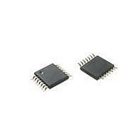
MCU AVR 2KB FLASH 12MHZ 14TSSOP
Manufacturer
Atmel
Series
AVR® ATtinyr
Datasheet
1.ATTINY20-EK1.pdf
(224 pages)
Specifications of ATTINY20-XU
Core Processor
AVR
Core Size
8-Bit
Speed
12MHz
Connectivity
I²C, SPI
Peripherals
Brown-out Detect/Reset, POR, PWM, WDT
Number Of I /o
12
Program Memory Size
2KB (1K x 16)
Program Memory Type
FLASH
Ram Size
128 x 8
Voltage - Supply (vcc/vdd)
1.8 V ~ 5.5 V
Data Converters
A/D 8x10b
Oscillator Type
Internal
Operating Temperature
-40°C ~ 85°C
Package / Case
*
Processor Series
ATtiny
Core
AVR
Data Bus Width
8 bit
Data Ram Size
128 B
Interface Type
SPI, TWI
Maximum Clock Frequency
12 MHz
Number Of Programmable I/os
12
Number Of Timers
2
Operating Supply Voltage
3.3 V
Maximum Operating Temperature
+ 85 C
Mounting Style
SMD/SMT
Minimum Operating Temperature
- 40 C
Operating Temperature Range
- 40 C to + 85 C
Lead Free Status / RoHS Status
Lead free / RoHS Compliant
Eeprom Size
-
Lead Free Status / Rohs Status
Details
Available stocks
Company
Part Number
Manufacturer
Quantity
Price
Company:

Part Number:
ATTINY20-XU
Manufacturer:
Atmel
Quantity:
904


130
ATtiny20
To enable the SPI module, the PRSPI bit in the Power Reduction Register must be written to
zero. See
The interconnection between Master and Slave CPUs with SPI is shown in
130. The system consists of two shift Registers, and a Master clock generator. The SPI Master
initiates the communication cycle when pulling low the Slave Select SS pin of the desired Slave.
Master and Slave prepare the data to be sent in their respective shift Registers, and the Master
generates the required clock pulses on the SCK line to interchange data. Data is always shifted
from Master to Slave on the Master Out – Slave In, MOSI, line, and from Slave to Master on the
Master In – Slave Out, MISO, line. After each data packet, the Master will synchronize the Slave
by pulling high the Slave Select, SS, line.
When configured as a Master, the SPI interface has no automatic control of the SS line. This
must be handled by user software before communication can start. When this is done, writing a
byte to the SPI Data Register starts the SPI clock generator, and the hardware shifts the eight
bits into the Slave. After shifting one byte, the SPI clock generator stops, setting the end of
Transmission Flag (SPIF). If the SPI Interrupt Enable bit (SPIE) in the SPCR Register is set, an
interrupt is requested. The Master may continue to shift the next byte by writing it into SPDR, or
signal the end of packet by pulling high the Slave Select, SS line. The last incoming byte will be
kept in the Buffer Register for later use.
When configured as a Slave, the SPI interface will remain sleeping with MISO tri-stated as long
as the SS pin is driven high. In this state, software may update the contents of the SPI Data
Register, SPDR, but the data will not be shifted out by incoming clock pulses on the SCK pin
until the SS pin is driven low. As one byte has been completely shifted, the end of Transmission
Flag, SPIF is set. If the SPI Interrupt Enable bit, SPIE, in the SPCR Register is set, an interrupt
is requested. The Slave may continue to place new data to be sent into SPDR before reading
the incoming data. The last incoming byte will be kept in the Buffer Register for later use.
Figure 16-2. SPI Master-Slave Interconnection
The system is single buffered in the transmit direction and double buffered in the receive direc-
tion. This means that bytes to be transmitted cannot be written to the SPI Data Register before
the entire shift cycle is completed. When receiving data, however, a received character must be
read from the SPI Data Register before the next character has been completely shifted in. Oth-
erwise, the first byte is lost.
In SPI Slave mode, the control logic will sample the incoming signal of the SCK pin. To ensure
correct sampling of the clock signal, the minimum low and high periods should be:
“PRR – Power Reduction Register” on page
29.
Figure 16-2 on page
8235B–AVR–04/11
SHIFT
ENABLE
Related parts for ATTINY20-XU
Image
Part Number
Description
Manufacturer
Datasheet
Request
R

Part Number:
Description:
IC, MCU, 8BIT, 2K FLASH, 20SOIC
Manufacturer:
Atmel
Datasheet:

Part Number:
Description:
IC, MCU, 8BIT, 2K FLASH, 20PDIP
Manufacturer:
Atmel
Datasheet:
Part Number:
Description:
IC, MCU, 8BIT, 8K FLASH, 20PDIP
Manufacturer:
Atmel
Datasheet:
Part Number:
Description:
IC, MCU, 8BIT, 8K FLASH, 20SOIC
Manufacturer:
Atmel
Datasheet:

Part Number:
Description:
DEV KIT FOR AVR/AVR32
Manufacturer:
Atmel
Datasheet:

Part Number:
Description:
INTERVAL AND WIPE/WASH WIPER CONTROL IC WITH DELAY
Manufacturer:
ATMEL Corporation
Datasheet:
Part Number:
Description:
Low-Voltage Voice-Switched IC for Hands-Free Operation
Manufacturer:
ATMEL Corporation
Datasheet:
Part Number:
Description:
MONOLITHIC INTEGRATED FEATUREPHONE CIRCUIT
Manufacturer:
ATMEL Corporation
Datasheet:
Part Number:
Description:
AM-FM Receiver IC U4255BM-M
Manufacturer:
ATMEL Corporation
Datasheet:
Part Number:
Description:
Monolithic Integrated Feature Phone Circuit
Manufacturer:
ATMEL Corporation
Datasheet:
Part Number:
Description:
Multistandard Video-IF and Quasi Parallel Sound Processing
Manufacturer:
ATMEL Corporation
Datasheet:
Part Number:
Description:
High-performance EE PLD
Manufacturer:
ATMEL Corporation
Datasheet: