ATTINY20-XU Atmel, ATTINY20-XU Datasheet - Page 19
ATTINY20-XU
Manufacturer Part Number
ATTINY20-XU
Description
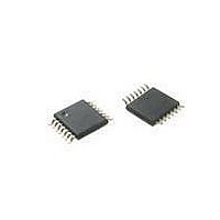
MCU AVR 2KB FLASH 12MHZ 14TSSOP
Manufacturer
Atmel
Series
AVR® ATtinyr
Datasheet
1.ATTINY20-EK1.pdf
(224 pages)
Specifications of ATTINY20-XU
Core Processor
AVR
Core Size
8-Bit
Speed
12MHz
Connectivity
I²C, SPI
Peripherals
Brown-out Detect/Reset, POR, PWM, WDT
Number Of I /o
12
Program Memory Size
2KB (1K x 16)
Program Memory Type
FLASH
Ram Size
128 x 8
Voltage - Supply (vcc/vdd)
1.8 V ~ 5.5 V
Data Converters
A/D 8x10b
Oscillator Type
Internal
Operating Temperature
-40°C ~ 85°C
Package / Case
*
Processor Series
ATtiny
Core
AVR
Data Bus Width
8 bit
Data Ram Size
128 B
Interface Type
SPI, TWI
Maximum Clock Frequency
12 MHz
Number Of Programmable I/os
12
Number Of Timers
2
Operating Supply Voltage
3.3 V
Maximum Operating Temperature
+ 85 C
Mounting Style
SMD/SMT
Minimum Operating Temperature
- 40 C
Operating Temperature Range
- 40 C to + 85 C
Lead Free Status / RoHS Status
Lead free / RoHS Compliant
Eeprom Size
-
Lead Free Status / Rohs Status
Details
Available stocks
Company
Part Number
Manufacturer
Quantity
Price
Company:

Part Number:
ATTINY20-XU
Manufacturer:
Atmel
Quantity:
904


6.1.4
6.2
6.2.1
6.2.2
8235B–AVR–04/11
Clock Sources
ADC Clock – clk
Calibrated Internal 8 MHz Oscillator
External Clock
The ADC is provided with a dedicated clock domain. This allows halting the CPU and I/O clocks
in order to reduce noise generated by digital circuitry. This gives more accurate ADC conversion
results.
All synchronous clock signals are derived from the main clock. The device has three alternative
sources for the main clock, as follows:
See
The calibrated internal oscillator provides an approximately 8 MHz clock signal. Though voltage
and temperature dependent, this clock can be very accurately calibrated by the user. See
20-2 on page
This clock may be selected as the main clock by setting the Clock Main Select bits CLKMS[1:0]
in CLKMSR to 0b00. Once enabled, the oscillator will operate with no external components. Dur-
ing reset, hardware loads the calibration byte into the OSCCAL register and thereby
automatically calibrates the oscillator. The accuracy of this calibration is shown as Factory cali-
bration in
When this oscillator is used as the main clock, the watchdog oscillator will still be used for the
watchdog timer and reset time-out. For more information on the pre-programmed calibration
value, see section
To use the device with an external clock source, CLKI should be driven as shown in
The external clock is selected as the main clock by setting CLKMS[1:0] bits in CLKMSR to 0b10.
Figure 6-2.
When applying an external clock, it is required to avoid sudden changes in the applied clock fre-
quency to ensure stable operation of the MCU. A variation in frequency of more than 2% from
one clock cycle to the next can lead to unpredictable behavior. It is required to ensure that the
MCU is kept in reset during such changes in the clock frequency.
ADC
• Calibrated Internal 8 MHz Oscillator (see
• External Clock (see
• Internal 128 kHz Oscillator (see
Table 6-3 on page 22
Table 20-2 on page
174, and
External Clock Drive Configuration
“Calibration Section” on page
“Internal Oscillator Speed” on page 205
page
on how to select and change the active clock source.
EXTERNAL
19)
174.
SIGNAL
CLOCK
page
20)
page
166.
19)
CLKI
GND
for more details.
ATtiny20
Figure
Table
6-2.
19
Related parts for ATTINY20-XU
Image
Part Number
Description
Manufacturer
Datasheet
Request
R

Part Number:
Description:
IC, MCU, 8BIT, 2K FLASH, 20SOIC
Manufacturer:
Atmel
Datasheet:

Part Number:
Description:
IC, MCU, 8BIT, 2K FLASH, 20PDIP
Manufacturer:
Atmel
Datasheet:
Part Number:
Description:
IC, MCU, 8BIT, 8K FLASH, 20PDIP
Manufacturer:
Atmel
Datasheet:
Part Number:
Description:
IC, MCU, 8BIT, 8K FLASH, 20SOIC
Manufacturer:
Atmel
Datasheet:

Part Number:
Description:
DEV KIT FOR AVR/AVR32
Manufacturer:
Atmel
Datasheet:

Part Number:
Description:
INTERVAL AND WIPE/WASH WIPER CONTROL IC WITH DELAY
Manufacturer:
ATMEL Corporation
Datasheet:
Part Number:
Description:
Low-Voltage Voice-Switched IC for Hands-Free Operation
Manufacturer:
ATMEL Corporation
Datasheet:
Part Number:
Description:
MONOLITHIC INTEGRATED FEATUREPHONE CIRCUIT
Manufacturer:
ATMEL Corporation
Datasheet:
Part Number:
Description:
AM-FM Receiver IC U4255BM-M
Manufacturer:
ATMEL Corporation
Datasheet:
Part Number:
Description:
Monolithic Integrated Feature Phone Circuit
Manufacturer:
ATMEL Corporation
Datasheet:
Part Number:
Description:
Multistandard Video-IF and Quasi Parallel Sound Processing
Manufacturer:
ATMEL Corporation
Datasheet:
Part Number:
Description:
High-performance EE PLD
Manufacturer:
ATMEL Corporation
Datasheet: