ATTINY20-XU Atmel, ATTINY20-XU Datasheet - Page 146
ATTINY20-XU
Manufacturer Part Number
ATTINY20-XU
Description
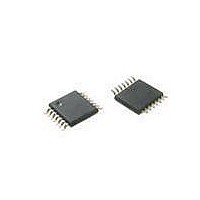
MCU AVR 2KB FLASH 12MHZ 14TSSOP
Manufacturer
Atmel
Series
AVR® ATtinyr
Datasheet
1.ATTINY20-EK1.pdf
(224 pages)
Specifications of ATTINY20-XU
Core Processor
AVR
Core Size
8-Bit
Speed
12MHz
Connectivity
I²C, SPI
Peripherals
Brown-out Detect/Reset, POR, PWM, WDT
Number Of I /o
12
Program Memory Size
2KB (1K x 16)
Program Memory Type
FLASH
Ram Size
128 x 8
Voltage - Supply (vcc/vdd)
1.8 V ~ 5.5 V
Data Converters
A/D 8x10b
Oscillator Type
Internal
Operating Temperature
-40°C ~ 85°C
Package / Case
*
Processor Series
ATtiny
Core
AVR
Data Bus Width
8 bit
Data Ram Size
128 B
Interface Type
SPI, TWI
Maximum Clock Frequency
12 MHz
Number Of Programmable I/os
12
Number Of Timers
2
Operating Supply Voltage
3.3 V
Maximum Operating Temperature
+ 85 C
Mounting Style
SMD/SMT
Minimum Operating Temperature
- 40 C
Operating Temperature Range
- 40 C to + 85 C
Lead Free Status / RoHS Status
Lead free / RoHS Compliant
Eeprom Size
-
Lead Free Status / Rohs Status
Details
Available stocks
Company
Part Number
Manufacturer
Quantity
Price
Company:

Part Number:
ATTINY20-XU
Manufacturer:
Atmel
Quantity:
904


17.4.1.2
17.4.1.3
17.4.1.4
17.4.2
17.4.3
17.5
17.5.1
146
Register Description
ATtiny20
Receiving Data Packets
Transmitting Data Packets
TWSCRA – TWI Slave Control Register A
Case 2: Address packet accepted - Direction bit cleared
Case 3: Collision
Case 4: STOP condition received.
If the R/W Direction flag is cleared this indicates a master write operation. The SCL line is forced
low, stretching the bus clock. If ACK is sent by the slave, the slave will wait for data to be
received. Data, Repeated START or STOP can be received after this. If NACK is indicated the
slave will wait for a new START condition and address match.
If the slave is not able to send a high level or NACK, the Collision flag is set and it will disable the
data and acknowledge output from the slave logic. The clock hold is released. A START or
repeated START condition will be accepted.
Operation is the same as case 1 or 2 above with one exception. When the STOP condition is
received, the Slave Address/Stop flag will be set indicating that a STOP condition and not an
address match occurred.
The slave will know when an address packet with R/W direction bit cleared has been success-
fully received. After acknowledging this, the slave must be ready to receive data. When a data
packet is received the Data Interrupt Flag is set, and the slave must indicate ACK or NACK.
After indicating a NACK, the slave must expect a STOP or Repeated START condition.
The slave will know when an address packet, with R/W direction bit set, has been successfully
received. It can then start sending data by writing to the Slave Data register. When a data packet
transmission is completed, the Data Interrupt Flag is set. If the master indicates NACK, the slave
must stop transmitting data, and expect a STOP or Repeated START condition.
• Bit 7 – TWSHE: TWI SDA Hold Time Enable
When this bit is set each negative transition of SCL triggers an additional internal delay, before
the device is allowed to change the SDA line. The added delay is approximately 50ns in length.
This may be useful in SMBus systems.
• Bit 6 – Res: Reserved Bit
This bit is reserved and will always read as zero.
• Bit 5 – TWDIE: TWI Data Interrupt Enable
When this bit is set and interrupts are enabled, a TWI interrupt will be generated when the data
interrupt flag (TWDIF) in TWSSRA is set.
Bit
0x2D
Read/Write
Initial Value
TWSHE
R/W
7
0
R
6
–
0
TWDIE
R/W
5
0
TWASIE
R/W
4
0
TWEN
R/W
3
0
TWSIE
R/W
2
0
TWPME
R/W
1
0
TWSME
R/W
0
0
8235B–AVR–04/11
TWSCRA
Related parts for ATTINY20-XU
Image
Part Number
Description
Manufacturer
Datasheet
Request
R

Part Number:
Description:
IC, MCU, 8BIT, 2K FLASH, 20SOIC
Manufacturer:
Atmel
Datasheet:

Part Number:
Description:
IC, MCU, 8BIT, 2K FLASH, 20PDIP
Manufacturer:
Atmel
Datasheet:
Part Number:
Description:
IC, MCU, 8BIT, 8K FLASH, 20PDIP
Manufacturer:
Atmel
Datasheet:
Part Number:
Description:
IC, MCU, 8BIT, 8K FLASH, 20SOIC
Manufacturer:
Atmel
Datasheet:

Part Number:
Description:
DEV KIT FOR AVR/AVR32
Manufacturer:
Atmel
Datasheet:

Part Number:
Description:
INTERVAL AND WIPE/WASH WIPER CONTROL IC WITH DELAY
Manufacturer:
ATMEL Corporation
Datasheet:
Part Number:
Description:
Low-Voltage Voice-Switched IC for Hands-Free Operation
Manufacturer:
ATMEL Corporation
Datasheet:
Part Number:
Description:
MONOLITHIC INTEGRATED FEATUREPHONE CIRCUIT
Manufacturer:
ATMEL Corporation
Datasheet:
Part Number:
Description:
AM-FM Receiver IC U4255BM-M
Manufacturer:
ATMEL Corporation
Datasheet:
Part Number:
Description:
Monolithic Integrated Feature Phone Circuit
Manufacturer:
ATMEL Corporation
Datasheet:
Part Number:
Description:
Multistandard Video-IF and Quasi Parallel Sound Processing
Manufacturer:
ATMEL Corporation
Datasheet:
Part Number:
Description:
High-performance EE PLD
Manufacturer:
ATMEL Corporation
Datasheet: