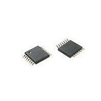
ATTINY20-XU Atmel, ATTINY20-XU Datasheet - Page 116

ATTINY20-XU
Manufacturer Part Number
ATTINY20-XU
Description
MCU AVR 2KB FLASH 12MHZ 14TSSOP
Manufacturer
Atmel
Series
AVR® ATtinyr
Datasheet
1.ATTINY20-EK1.pdf
(224 pages)
Specifications of ATTINY20-XU
Core Processor
AVR
Core Size
8-Bit
Speed
12MHz
Connectivity
I²C, SPI
Peripherals
Brown-out Detect/Reset, POR, PWM, WDT
Number Of I /o
12
Program Memory Size
2KB (1K x 16)
Program Memory Type
FLASH
Ram Size
128 x 8
Voltage - Supply (vcc/vdd)
1.8 V ~ 5.5 V
Data Converters
A/D 8x10b
Oscillator Type
Internal
Operating Temperature
-40°C ~ 85°C
Package / Case
*
Processor Series
ATtiny
Core
AVR
Data Bus Width
8 bit
Data Ram Size
128 B
Interface Type
SPI, TWI
Maximum Clock Frequency
12 MHz
Number Of Programmable I/os
12
Number Of Timers
2
Operating Supply Voltage
3.3 V
Maximum Operating Temperature
+ 85 C
Mounting Style
SMD/SMT
Minimum Operating Temperature
- 40 C
Operating Temperature Range
- 40 C to + 85 C
Lead Free Status / RoHS Status
Lead free / RoHS Compliant
Eeprom Size
-
Lead Free Status / Rohs Status
Details
Available stocks
Company
Part Number
Manufacturer
Quantity
Price
Company:
Part Number:
ATTINY20-XU
Manufacturer:
Atmel
Quantity:
904
- Current page: 116 of 224
- Download datasheet (6Mb)
116
ATtiny20
prescaling is set by the ADPS bits in ADCSRA. The prescaler starts counting from the moment
the ADC is switched on by setting the ADEN bit in ADCSRA. The prescaler keeps running for as
long as the ADEN bit is set, and is continuously reset when ADEN is low.
When initiating a single ended conversion by setting the ADSC bit in ADCSRA, the conversion
starts at the following rising edge of the ADC clock cycle.
A normal conversion takes 13 ADC clock cycles, as summarised in
first conversion after the ADC is switched on (ADEN in ADCSRA is set) takes 25 ADC clock
cycles in order to initialize the analog circuitry, as shown in
Figure 15-4. ADC Timing Diagram, First Conversion (Single Conversion Mode)
The actual sample-and-hold takes place 1.5 ADC clock cycles after the start of a normal conver-
sion and 13.5 ADC clock cycles after the start of a first conversion. See
conversion is complete, the result is written to the ADC Data Registers, and ADIF is set. In Sin-
gle Conversion mode, ADSC is cleared simultaneously. The software may then set ADSC again,
and a new conversion will be initiated on the first rising ADC clock edge.
Figure 15-5. ADC Timing Diagram, Single Conversion
When Auto Triggering is used, the prescaler is reset when the trigger event occurs, as shown in
Figure 15-6
Cycle Number
ADC Clock
ADEN
ADSC
ADIF
ADCH
ADCL
Cycle Number
ADC Clock
ADSC
ADIF
ADCH
ADCL
below. This assures a fixed delay from the trigger event to the start of conversion. In
1
1
2
MUX and REFS
Update
2
MUX and REFS
Update
12
3
13
Sample & Hold
4
14
5
15
6
Sample & Hold
16
First Conversion
17
7
One Conversion
18
8
19
9
20
10
Conversion
Complete
21
Figure 15-4
11
22
Conversion
Complete
23
12
Table 15-1 on page
24
13
below.
25
Figure
Sign and MSB of Result
Sign and MSB of Result
LSB of Result
Next Conversion
1
Next
Conversion
1
LSB of Result
15-5. When a
8235B–AVR–04/11
2
MUX and REFS
Update
2
MUX and REFS
Update
118. The
3
3
Related parts for ATTINY20-XU
Image
Part Number
Description
Manufacturer
Datasheet
Request
R

Part Number:
Description:
IC, MCU, 8BIT, 2K FLASH, 20SOIC
Manufacturer:
Atmel
Datasheet:

Part Number:
Description:
IC, MCU, 8BIT, 2K FLASH, 20PDIP
Manufacturer:
Atmel
Datasheet:

Part Number:
Description:
IC, MCU, 8BIT, 8K FLASH, 20PDIP
Manufacturer:
Atmel
Datasheet:

Part Number:
Description:
IC, MCU, 8BIT, 8K FLASH, 20SOIC
Manufacturer:
Atmel
Datasheet:

Part Number:
Description:
DEV KIT FOR AVR/AVR32
Manufacturer:
Atmel
Datasheet:

Part Number:
Description:
INTERVAL AND WIPE/WASH WIPER CONTROL IC WITH DELAY
Manufacturer:
ATMEL Corporation
Datasheet:

Part Number:
Description:
Low-Voltage Voice-Switched IC for Hands-Free Operation
Manufacturer:
ATMEL Corporation
Datasheet:

Part Number:
Description:
MONOLITHIC INTEGRATED FEATUREPHONE CIRCUIT
Manufacturer:
ATMEL Corporation
Datasheet:

Part Number:
Description:
AM-FM Receiver IC U4255BM-M
Manufacturer:
ATMEL Corporation
Datasheet:

Part Number:
Description:
Monolithic Integrated Feature Phone Circuit
Manufacturer:
ATMEL Corporation
Datasheet:

Part Number:
Description:
Multistandard Video-IF and Quasi Parallel Sound Processing
Manufacturer:
ATMEL Corporation
Datasheet:

Part Number:
Description:
High-performance EE PLD
Manufacturer:
ATMEL Corporation
Datasheet:


