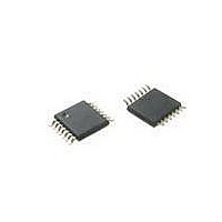
ATTINY20-XU Atmel, ATTINY20-XU Datasheet - Page 56

ATTINY20-XU
Manufacturer Part Number
ATTINY20-XU
Description
MCU AVR 2KB FLASH 12MHZ 14TSSOP
Manufacturer
Atmel
Series
AVR® ATtinyr
Datasheet
1.ATTINY20-EK1.pdf
(224 pages)
Specifications of ATTINY20-XU
Core Processor
AVR
Core Size
8-Bit
Speed
12MHz
Connectivity
I²C, SPI
Peripherals
Brown-out Detect/Reset, POR, PWM, WDT
Number Of I /o
12
Program Memory Size
2KB (1K x 16)
Program Memory Type
FLASH
Ram Size
128 x 8
Voltage - Supply (vcc/vdd)
1.8 V ~ 5.5 V
Data Converters
A/D 8x10b
Oscillator Type
Internal
Operating Temperature
-40°C ~ 85°C
Package / Case
*
Processor Series
ATtiny
Core
AVR
Data Bus Width
8 bit
Data Ram Size
128 B
Interface Type
SPI, TWI
Maximum Clock Frequency
12 MHz
Number Of Programmable I/os
12
Number Of Timers
2
Operating Supply Voltage
3.3 V
Maximum Operating Temperature
+ 85 C
Mounting Style
SMD/SMT
Minimum Operating Temperature
- 40 C
Operating Temperature Range
- 40 C to + 85 C
Lead Free Status / RoHS Status
Lead free / RoHS Compliant
Eeprom Size
-
Lead Free Status / Rohs Status
Details
Available stocks
Company
Part Number
Manufacturer
Quantity
Price
Company:
Part Number:
ATTINY20-XU
Manufacturer:
Atmel
Quantity:
904
- Current page: 56 of 224
- Download datasheet (6Mb)
56
ATtiny20
• Port B, Bit 0 – T0/CLKI/TPICLK/PCINT8
• Port B, Bit 1 – OC1A/SDA/MOSI/TPIDATA/PCINT9
• Port B, Bit 2 – INT0/OC0A/OC1B/MISO/CKOUT/PCINT10
• Port B, Bit 3 – RESET/PCINT11
• T0: Timer/Counter0 Clock Source.
• CLKI: Clock Input from an external clock source, see
• TPICLK: Serial Programming Clock.
• PCINT8: Pin Change Interrupt source 8. The PB0 pin can serve as an external interrupt
• OC1A: Output Compare Match output. Provided that the pin has been configured as an
• SDA: TWI Data. The pin is disconnected from the port and becomes the serial data for the
• MOSI: SPI Master Output / Slave Input. Regardless of DDB1, this pin is automatically
• TPIDATA: Serial Programming Data.
• PCINT9: Pin Change Interrupt source 9. The PB1 pin can serve as an external interrupt
• INT0: External Interrupt Request 0.
• OC0A: Output Compare Match output. Provided that the pin has been configured as an
• OC1B: Output Compare Match output. Provided that the pin has been configured as an
• MISO: SPI Master Input / Slave Output. Regardless of DDB2, this pin is automatically
• CKOUT - System Clock Output: The system clock can be output on the PB2 pin. The system
• PCINT10: Pin Change Interrupt source 10. The PB2 pin can serve as an external interrupt
• RESET: External Reset input is active low and enabled by unprogramming (“1”) the
• PCINT11: Pin Change Interrupt source 11. The PB3 pin can serve as an external interrupt
source for pin change interrupt 1.
output it serves as an external output for Timer/Counter1 Compare Match A. This pin is also
the output for the timer/counter PWM mode function.
TWI when TWEN in TWSCRA is set. In this mode of operation, the pin is driven by an open
drain driver with slew rate limitation and a spike filter.
configured as an input when SPI is enabled as a slave. The data direction of this pin is
controlled by DDB1 when SPI is enabled as a master.
source for pin change interrupt 1.
output it serves as an external output for Timer/Counter0 Compare Match A. This pin is also
the output for the timer/counter PWM mode function.
output it serves as an external output for Timer/Counter1 Compare Match B. This pin is also
the output for the timer/counter PWM mode function.
configured as an input when SPI is enabled as a master. The data direction of this pin is
controlled by DDB2 when SPI is enabled as a slave.
clock will be output if the CKOUT Fuse is programmed, regardless of the PORTB2 and DDB2
settings. It will also be output during reset.
source for pin change interrupt 1.
RSTDISBL Fuse. Pullup is activated and output driver and digital input are deactivated when
the pin is used as the RESET pin.
source for pin change interrupt 1.
“External Clock” on page
19.
8235B–AVR–04/11
Related parts for ATTINY20-XU
Image
Part Number
Description
Manufacturer
Datasheet
Request
R

Part Number:
Description:
IC, MCU, 8BIT, 2K FLASH, 20SOIC
Manufacturer:
Atmel
Datasheet:

Part Number:
Description:
IC, MCU, 8BIT, 2K FLASH, 20PDIP
Manufacturer:
Atmel
Datasheet:

Part Number:
Description:
IC, MCU, 8BIT, 8K FLASH, 20PDIP
Manufacturer:
Atmel
Datasheet:

Part Number:
Description:
IC, MCU, 8BIT, 8K FLASH, 20SOIC
Manufacturer:
Atmel
Datasheet:

Part Number:
Description:
DEV KIT FOR AVR/AVR32
Manufacturer:
Atmel
Datasheet:

Part Number:
Description:
INTERVAL AND WIPE/WASH WIPER CONTROL IC WITH DELAY
Manufacturer:
ATMEL Corporation
Datasheet:

Part Number:
Description:
Low-Voltage Voice-Switched IC for Hands-Free Operation
Manufacturer:
ATMEL Corporation
Datasheet:

Part Number:
Description:
MONOLITHIC INTEGRATED FEATUREPHONE CIRCUIT
Manufacturer:
ATMEL Corporation
Datasheet:

Part Number:
Description:
AM-FM Receiver IC U4255BM-M
Manufacturer:
ATMEL Corporation
Datasheet:

Part Number:
Description:
Monolithic Integrated Feature Phone Circuit
Manufacturer:
ATMEL Corporation
Datasheet:

Part Number:
Description:
Multistandard Video-IF and Quasi Parallel Sound Processing
Manufacturer:
ATMEL Corporation
Datasheet:

Part Number:
Description:
High-performance EE PLD
Manufacturer:
ATMEL Corporation
Datasheet:


