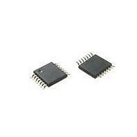
ATTINY20-XU Atmel, ATTINY20-XU Datasheet - Page 144

ATTINY20-XU
Manufacturer Part Number
ATTINY20-XU
Description
MCU AVR 2KB FLASH 12MHZ 14TSSOP
Manufacturer
Atmel
Series
AVR® ATtinyr
Datasheet
1.ATTINY20-EK1.pdf
(224 pages)
Specifications of ATTINY20-XU
Core Processor
AVR
Core Size
8-Bit
Speed
12MHz
Connectivity
I²C, SPI
Peripherals
Brown-out Detect/Reset, POR, PWM, WDT
Number Of I /o
12
Program Memory Size
2KB (1K x 16)
Program Memory Type
FLASH
Ram Size
128 x 8
Voltage - Supply (vcc/vdd)
1.8 V ~ 5.5 V
Data Converters
A/D 8x10b
Oscillator Type
Internal
Operating Temperature
-40°C ~ 85°C
Package / Case
*
Processor Series
ATtiny
Core
AVR
Data Bus Width
8 bit
Data Ram Size
128 B
Interface Type
SPI, TWI
Maximum Clock Frequency
12 MHz
Number Of Programmable I/os
12
Number Of Timers
2
Operating Supply Voltage
3.3 V
Maximum Operating Temperature
+ 85 C
Mounting Style
SMD/SMT
Minimum Operating Temperature
- 40 C
Operating Temperature Range
- 40 C to + 85 C
Lead Free Status / RoHS Status
Lead free / RoHS Compliant
Eeprom Size
-
Lead Free Status / Rohs Status
Details
Available stocks
Company
Part Number
Manufacturer
Quantity
Price
Company:
Part Number:
ATTINY20-XU
Manufacturer:
Atmel
Quantity:
904
- Current page: 144 of 224
- Download datasheet (6Mb)
17.3.10
17.4
144
TWI Slave Operation
ATtiny20
Compatibility with SMBus
Figure 17-10. Clock Synchronization
A high to low transition on the SCL line will force the line low for all masters on the bus and they
start timing their low clock period. The timing length of the low clock period can vary between the
masters. When a master (DEVICE1 in this case) has completed its low period it releases the
SCL line. However, the SCL line will not go high before all masters have released it. Conse-
quently the SCL line will be held low by the device with the longest low period (DEVICE2).
Devices with shorter low periods must insert a wait-state until the clock is released. All masters
start their high period when the SCL line is released by all devices and has become high. The
device which first completes its high period (DEVICE1) forces the clock line low and the proce-
dure are then repeated. The result of this is that the device with the shortest clock period
determines the high period while the low period of the clock is determined by the longest clock
period.
As with any other I
should be aware of before connecting a TWI device to SMBus devices. For use in SMBus envi-
ronments, the following should be noted:
The TWI slave is byte-oriented with optional interrupts after each byte. There are separate inter-
rupt flags for Data Interrupt and Address/Stop Interrupt. Interrupt flags can be set to trigger the
• All I/O pins of an AVR, including those of the two-wire interface, have protection diodes to
• The data hold time of the TWI is lower than specified for SMBus. The TWSHE bit of
• SMBus has a low speed limit, while I
both supply voltage and ground. See
requirements of the SMBus specifications. As a result, supply voltage mustn’t be removed
from the AVR or the protection diodes will pull the bus lines down. Power down and sleep
modes is not a problem, provided supply voltages remain.
TWSCRA can be used to increase the hold time. See
Register A” on page
AVR must make sure bus speed does not drop below specifications, since lower bus speeds
trigger timeouts in SMBus slaves. If the AVR is configured a slave there is a possibility of a
bus lockup, since the TWI module doesn't identify timeouts.
2
C-compliant interface there are known compatibility issues the designer
146.
2
Figure 10-1 on page
C hasn’t. As a master in an SMBus environment, the
“TWSCRA – TWI Slave Control
44. This is in contradiction to the
8235B–AVR–04/11
Related parts for ATTINY20-XU
Image
Part Number
Description
Manufacturer
Datasheet
Request
R

Part Number:
Description:
IC, MCU, 8BIT, 2K FLASH, 20SOIC
Manufacturer:
Atmel
Datasheet:

Part Number:
Description:
IC, MCU, 8BIT, 2K FLASH, 20PDIP
Manufacturer:
Atmel
Datasheet:

Part Number:
Description:
IC, MCU, 8BIT, 8K FLASH, 20PDIP
Manufacturer:
Atmel
Datasheet:

Part Number:
Description:
IC, MCU, 8BIT, 8K FLASH, 20SOIC
Manufacturer:
Atmel
Datasheet:

Part Number:
Description:
DEV KIT FOR AVR/AVR32
Manufacturer:
Atmel
Datasheet:

Part Number:
Description:
INTERVAL AND WIPE/WASH WIPER CONTROL IC WITH DELAY
Manufacturer:
ATMEL Corporation
Datasheet:

Part Number:
Description:
Low-Voltage Voice-Switched IC for Hands-Free Operation
Manufacturer:
ATMEL Corporation
Datasheet:

Part Number:
Description:
MONOLITHIC INTEGRATED FEATUREPHONE CIRCUIT
Manufacturer:
ATMEL Corporation
Datasheet:

Part Number:
Description:
AM-FM Receiver IC U4255BM-M
Manufacturer:
ATMEL Corporation
Datasheet:

Part Number:
Description:
Monolithic Integrated Feature Phone Circuit
Manufacturer:
ATMEL Corporation
Datasheet:

Part Number:
Description:
Multistandard Video-IF and Quasi Parallel Sound Processing
Manufacturer:
ATMEL Corporation
Datasheet:

Part Number:
Description:
High-performance EE PLD
Manufacturer:
ATMEL Corporation
Datasheet:


