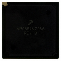
MPC564MZP56 Freescale Semiconductor, MPC564MZP56 Datasheet - Page 883

MPC564MZP56
Manufacturer Part Number
MPC564MZP56
Description
IC MCU 512K FLASH 56MHZ 388-BGA
Manufacturer
Freescale Semiconductor
Series
MPC5xxr
Specifications of MPC564MZP56
Core Processor
PowerPC
Core Size
32-Bit
Speed
56MHz
Connectivity
CAN, EBI/EMI, SCI, SPI, UART/USART
Peripherals
POR, PWM, WDT
Number Of I /o
56
Program Memory Size
512KB (512K x 8)
Program Memory Type
FLASH
Ram Size
32K x 8
Voltage - Supply (vcc/vdd)
2.5 V ~ 2.7 V
Data Converters
A/D 32x10b
Oscillator Type
External
Operating Temperature
-40°C ~ 125°C
Package / Case
388-BGA
Core
PowerPC
Processor Series
MPC5xx
Data Bus Width
32 bit
Maximum Clock Frequency
56 MHz
Data Ram Size
32 KB
On-chip Adc
Yes
Number Of Programmable I/os
56
Number Of Timers
2
Operating Supply Voltage
0 V to 5 V
Mounting Style
SMD/SMT
A/d Bit Size
10 bit
A/d Channels Available
32
Height
1.95 mm
Interface Type
CAN, JTAG, QSPI, SCI, SPI, UART
Length
27 mm
Maximum Operating Temperature
+ 125 C
Minimum Operating Temperature
- 40 C
Supply Voltage (max)
2.7 V, 5.25 V
Supply Voltage (min)
2.5 V, 4.75 V
Width
27 mm
For Use With
MPC564EVB - KIT EVAL FOR MPC561/562/563/564
Lead Free Status / RoHS Status
Contains lead / RoHS non-compliant
Eeprom Size
-
Lead Free Status / Rohs Status
No RoHS Version Available
Available stocks
Company
Part Number
Manufacturer
Quantity
Price
Company:
Part Number:
MPC564MZP56
Manufacturer:
FREESCAL
Quantity:
364
Company:
Part Number:
MPC564MZP56
Manufacturer:
Freescale Semiconductor
Quantity:
10 000
Part Number:
MPC564MZP56
Manufacturer:
FREESCALE
Quantity:
20 000
Company:
Part Number:
MPC564MZP56R2
Manufacturer:
Freescale Semiconductor
Quantity:
10 000
- Current page: 883 of 1420
- Download datasheet (11Mb)
21.3.3.1
An internal address comparator is used to determine if addressed information is stored in a read page
buffer. If the address of a read access matches data contained in a read page buffer, that addressed data is
transferred from the read page buffer to the data bus. An off-page read access to transfer data from the
Flash array to the data bus is not performed in this case.
21.3.4
The normal array is accessed when the SIE register bit in the UC3FMCR = 0. When SIE = 1, reads to the
array access the shadow information row.
21.3.5
The only valid writes to the UC3F array are program or erase interlock writes. In the case of program
interlock writes, the address of the write determines the location to be programmed while the data written
is transferred to the program data latches to be programmed into the array. Address and data written during
an erase interlock write is a “don’t care” and is not stored anywhere.
21.3.6
There are two fundamental high voltage operations, program and erase. Program changes a UC3F array
bitcell from a logic 1 state to a logic 0 state and is a selective operation performed on up to 32 bits at a
time. Erase changes a UC3F array bitcell from a logic 0 state to a logic 1 state and is a bulk operation
performed on one block or multiple blocks of the UC3F array.
21.3.6.1
The embedded hardware program/erase algorithm relies on an internal state machine to perform the
program and erase sequences. The embedded hardware algorithm uses an internal oscillator to control the
high voltage pulse duration and hardware control logic. The embedded hardware algorithm is also
responsible for performing all margin reads and applying high voltage pulses to ensure each bit is
programmed or erased with sufficient margin. Upon successful program or erase operation, the
program/erase hardware control logic terminates the program or erase operation with a pass status
(PEGOOD = 1). The program/erase control logic will time out in the event that the maximum program or
erase time is exceeded and return a fail status (PEGOOD = 0).
21.3.7
To modify the charge stored in an isolated element of the UC3F bit from a logic 1 state to a logic 0 state,
a programming operation is required. This programming operation applies the required voltages to change
the charge state of the selected bits without changing the logic state of any other bits in the UC3F array.
The program operation cannot change the logic 0 state to a logic 1 state; this transition must be done by
the erase operation. Programming uses a program data latch to store the data to be programmed and an
address latch to store the word address to be programmed. The UC3F Array may be programmed by byte
(8 bits), half-word (16 bits), or word (32 bits).
Freescale Semiconductor
Shadow Row Select Read Operation
Array Program/Erase Interlock Write Operation
High Voltage Operations
Programming
Array On-Page Read Operation
Overview of Program/Erase Operation
MPC561/MPC563 Reference Manual, Rev. 1.2
CDR3 Flash (UC3F) EEPROM
21-21
Related parts for MPC564MZP56
Image
Part Number
Description
Manufacturer
Datasheet
Request
R

Part Number:
Description:
MPC5 1K0 5%
Manufacturer:
TE Connectivity
Datasheet:

Part Number:
Description:
MPC5 500R 5%
Manufacturer:
TE Connectivity
Datasheet:

Part Number:
Description:
MPC5 5K0 5%
Manufacturer:
Tyco Electronics
Datasheet:

Part Number:
Description:
MPC5 5R0 5%
Manufacturer:
Tyco Electronics
Datasheet:

Part Number:
Description:
MPC5 50K 5%
Manufacturer:
Tyco Electronics
Datasheet:

Part Number:
Description:
MPC5 1R0 5%
Manufacturer:
Tyco Electronics
Datasheet:
Part Number:
Description:
Manufacturer:
Freescale Semiconductor, Inc
Datasheet:
Part Number:
Description:
Manufacturer:
Freescale Semiconductor, Inc
Datasheet:
Part Number:
Description:
Manufacturer:
Freescale Semiconductor, Inc
Datasheet:
Part Number:
Description:
Manufacturer:
Freescale Semiconductor, Inc
Datasheet:
Part Number:
Description:
Manufacturer:
Freescale Semiconductor, Inc
Datasheet:


