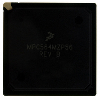
MPC564MZP56 Freescale Semiconductor, MPC564MZP56 Datasheet - Page 348

MPC564MZP56
Manufacturer Part Number
MPC564MZP56
Description
IC MCU 512K FLASH 56MHZ 388-BGA
Manufacturer
Freescale Semiconductor
Series
MPC5xxr
Specifications of MPC564MZP56
Core Processor
PowerPC
Core Size
32-Bit
Speed
56MHz
Connectivity
CAN, EBI/EMI, SCI, SPI, UART/USART
Peripherals
POR, PWM, WDT
Number Of I /o
56
Program Memory Size
512KB (512K x 8)
Program Memory Type
FLASH
Ram Size
32K x 8
Voltage - Supply (vcc/vdd)
2.5 V ~ 2.7 V
Data Converters
A/D 32x10b
Oscillator Type
External
Operating Temperature
-40°C ~ 125°C
Package / Case
388-BGA
Core
PowerPC
Processor Series
MPC5xx
Data Bus Width
32 bit
Maximum Clock Frequency
56 MHz
Data Ram Size
32 KB
On-chip Adc
Yes
Number Of Programmable I/os
56
Number Of Timers
2
Operating Supply Voltage
0 V to 5 V
Mounting Style
SMD/SMT
A/d Bit Size
10 bit
A/d Channels Available
32
Height
1.95 mm
Interface Type
CAN, JTAG, QSPI, SCI, SPI, UART
Length
27 mm
Maximum Operating Temperature
+ 125 C
Minimum Operating Temperature
- 40 C
Supply Voltage (max)
2.7 V, 5.25 V
Supply Voltage (min)
2.5 V, 4.75 V
Width
27 mm
For Use With
MPC564EVB - KIT EVAL FOR MPC561/562/563/564
Lead Free Status / RoHS Status
Contains lead / RoHS non-compliant
Eeprom Size
-
Lead Free Status / Rohs Status
No RoHS Version Available
Available stocks
Company
Part Number
Manufacturer
Quantity
Price
Company:
Part Number:
MPC564MZP56
Manufacturer:
FREESCAL
Quantity:
364
Company:
Part Number:
MPC564MZP56
Manufacturer:
Freescale Semiconductor
Quantity:
10 000
Part Number:
MPC564MZP56
Manufacturer:
FREESCALE
Quantity:
20 000
Company:
Part Number:
MPC564MZP56R2
Manufacturer:
Freescale Semiconductor
Quantity:
10 000
- Current page: 348 of 1420
- Download datasheet (11Mb)
External Bus Interface
9.5
This section provides a functional description of the system bus, the signals that control it, and the bus
cycles provided for data transfer operations. It also describes the error conditions, bus arbitration, and reset
operation.
The MPC561/MPC563 generates a system clock output (CLKOUT). This output sets the frequency of
operation for the bus interface directly. Internally, the MPC561/MPC563 uses a phase-lock loop (PLL)
circuit to generate a master clock for all of the MPC561/MPC563 circuitry (including the bus interface)
which is phase-locked to the CLKOUT output signal.
All signals for the MPC561/MPC563 bus interface are specified with respect to the rising edge of the
external CLKOUT and are guaranteed to be sampled as inputs or changed as outputs with respect to that
edge. Since the same clock edge is referenced for driving or sampling the bus signals, the possibility of
clock skew could exist between various modules in a system due to routing or the use of multiple clock
lines. It is the responsibility of the system to handle any such clock skew problems that could occur.
9.5.1
The basic transfer protocol defines the sequence of actions that must occur on the MPC561/MPC563 bus
to perform a complete bus transaction. A simplified scheme of the basic transfer protocol is illustrated in
Figure
The basic transfer protocol provides for an arbitration phase and an address and data transfer phase. The
address phase specifies the address for the transaction and the transfer attributes that describe the
transaction. The data phase performs the transfer of data (if any is to be transferred). The data phase may
transfer a single beat of data (four bytes or less) for nonburst operations, a 4-beat burst of data (4 x 4 bytes),
an 8-beat burst of data (8 x 2 bytes) or a 16-beat burst of data (16 x 1 bytes).
9-8
9-3.
Bus Operations
Signal Name
Basic Transfer Protocol
Arbitration
RETRY
Retry
Table 9-1. MPC561/MPC563 BIU Signals (continued)
Pins
1
MPC561/MPC563 Reference Manual, Rev. 1.2
Address Transfer
Figure 9-3. Basic Transfer Protocol
Active
Low
I/O
O
I
In the case of regular transaction, this signal is driven
by the slave device to indicate that the
MPC561/MPC563 must relinquish the ownership of
the bus and retry the cycle.
When an external master owns the bus and the
internal MPC561/MPC563 bus initiates access to the
external bus at the same time, this signal is used to
cause the external master to relinquish the bus for one
clock to solve the contention.
Data Transfer
Description
Termination
Freescale Semiconductor
Related parts for MPC564MZP56
Image
Part Number
Description
Manufacturer
Datasheet
Request
R

Part Number:
Description:
MPC5 1K0 5%
Manufacturer:
TE Connectivity
Datasheet:

Part Number:
Description:
MPC5 500R 5%
Manufacturer:
TE Connectivity
Datasheet:

Part Number:
Description:
MPC5 5K0 5%
Manufacturer:
Tyco Electronics
Datasheet:

Part Number:
Description:
MPC5 5R0 5%
Manufacturer:
Tyco Electronics
Datasheet:

Part Number:
Description:
MPC5 50K 5%
Manufacturer:
Tyco Electronics
Datasheet:

Part Number:
Description:
MPC5 1R0 5%
Manufacturer:
Tyco Electronics
Datasheet:
Part Number:
Description:
Manufacturer:
Freescale Semiconductor, Inc
Datasheet:
Part Number:
Description:
Manufacturer:
Freescale Semiconductor, Inc
Datasheet:
Part Number:
Description:
Manufacturer:
Freescale Semiconductor, Inc
Datasheet:
Part Number:
Description:
Manufacturer:
Freescale Semiconductor, Inc
Datasheet:
Part Number:
Description:
Manufacturer:
Freescale Semiconductor, Inc
Datasheet:


