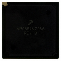
MPC564MZP56 Freescale Semiconductor, MPC564MZP56 Datasheet - Page 810

MPC564MZP56
Manufacturer Part Number
MPC564MZP56
Description
IC MCU 512K FLASH 56MHZ 388-BGA
Manufacturer
Freescale Semiconductor
Series
MPC5xxr
Specifications of MPC564MZP56
Core Processor
PowerPC
Core Size
32-Bit
Speed
56MHz
Connectivity
CAN, EBI/EMI, SCI, SPI, UART/USART
Peripherals
POR, PWM, WDT
Number Of I /o
56
Program Memory Size
512KB (512K x 8)
Program Memory Type
FLASH
Ram Size
32K x 8
Voltage - Supply (vcc/vdd)
2.5 V ~ 2.7 V
Data Converters
A/D 32x10b
Oscillator Type
External
Operating Temperature
-40°C ~ 125°C
Package / Case
388-BGA
Core
PowerPC
Processor Series
MPC5xx
Data Bus Width
32 bit
Maximum Clock Frequency
56 MHz
Data Ram Size
32 KB
On-chip Adc
Yes
Number Of Programmable I/os
56
Number Of Timers
2
Operating Supply Voltage
0 V to 5 V
Mounting Style
SMD/SMT
A/d Bit Size
10 bit
A/d Channels Available
32
Height
1.95 mm
Interface Type
CAN, JTAG, QSPI, SCI, SPI, UART
Length
27 mm
Maximum Operating Temperature
+ 125 C
Minimum Operating Temperature
- 40 C
Supply Voltage (max)
2.7 V, 5.25 V
Supply Voltage (min)
2.5 V, 4.75 V
Width
27 mm
For Use With
MPC564EVB - KIT EVAL FOR MPC561/562/563/564
Lead Free Status / RoHS Status
Contains lead / RoHS non-compliant
Eeprom Size
-
Lead Free Status / Rohs Status
No RoHS Version Available
Available stocks
Company
Part Number
Manufacturer
Quantity
Price
Company:
Part Number:
MPC564MZP56
Manufacturer:
FREESCAL
Quantity:
364
Company:
Part Number:
MPC564MZP56
Manufacturer:
Freescale Semiconductor
Quantity:
10 000
Part Number:
MPC564MZP56
Manufacturer:
FREESCALE
Quantity:
20 000
Company:
Part Number:
MPC564MZP56R2
Manufacturer:
Freescale Semiconductor
Quantity:
10 000
- Current page: 810 of 1420
- Download datasheet (11Mb)
Peripheral Pin Multiplexing (PPM) Module
18.3.1.1
In the MPC561/MPC563 devices, the PPM module supports multiplexing of four modules: TPU3_A,
TPU3_B, MIOS and GPIO registers, internal to the PPM. Internal multiplexers route data between the
MCU internal modules and the external device through the PPM. Four configuration registers,
TX_CONFIG_1, TX_CONFIG_2, RX_CONFIG_1 and RX_CONFIG_2, control these internal
multiplexers. By programming the configuration registers the PPM multiplexers select which internal
module will drive data out of the PPM and which will receive data from the PPM.
The TX_CONFIG and RX_CONFIG registers allocate two bits to control each of the 16 internal
multiplexers. During transmit operations, the TX_CONFIG registers determine which internal module’s
data will be sampled and routed to the transmit sample-and-shift register, TX_DATA. During receive
operations, data in the receive sample-and-shift register, RX_SHIFTER, is routed to the internal module
specified by the value of the RX_CONFIG registers, or in the case where GPDI is the destination, data is
routed directly from PPM_RX[0:1]. Refer to
18-4
IMB3 interface
TPU3_B
TPU3_A
MIOS
(GPDO, GPDI)
Internal Multiplexing
GPIO
PPM Module
Figure 18-2. Block Diagram of PPM Module
MPC561/MPC563 Reference Manual, Rev. 1.2
PPM_REGS
PPM_SHORT
PPM_MUX
Figure
Channel_TX[15:0]
Channel_RX[15:0]
18-4.
SYSCLK
Clock Generator
TCLK and Update
PPM_SHIFTER
Generator
Clock
Clock
Freescale Semiconductor
SYSCLK
PPM_TCLK
PPM_TSYNC
PPM_TX[0:1]
PPM_RX[0:1]
Related parts for MPC564MZP56
Image
Part Number
Description
Manufacturer
Datasheet
Request
R

Part Number:
Description:
MPC5 1K0 5%
Manufacturer:
TE Connectivity
Datasheet:

Part Number:
Description:
MPC5 500R 5%
Manufacturer:
TE Connectivity
Datasheet:

Part Number:
Description:
MPC5 5K0 5%
Manufacturer:
Tyco Electronics
Datasheet:

Part Number:
Description:
MPC5 5R0 5%
Manufacturer:
Tyco Electronics
Datasheet:

Part Number:
Description:
MPC5 50K 5%
Manufacturer:
Tyco Electronics
Datasheet:

Part Number:
Description:
MPC5 1R0 5%
Manufacturer:
Tyco Electronics
Datasheet:
Part Number:
Description:
Manufacturer:
Freescale Semiconductor, Inc
Datasheet:
Part Number:
Description:
Manufacturer:
Freescale Semiconductor, Inc
Datasheet:
Part Number:
Description:
Manufacturer:
Freescale Semiconductor, Inc
Datasheet:
Part Number:
Description:
Manufacturer:
Freescale Semiconductor, Inc
Datasheet:
Part Number:
Description:
Manufacturer:
Freescale Semiconductor, Inc
Datasheet:


