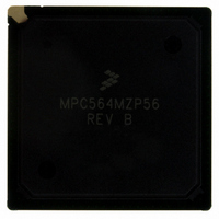
MPC564MZP56 Freescale Semiconductor, MPC564MZP56 Datasheet - Page 426

MPC564MZP56
Manufacturer Part Number
MPC564MZP56
Description
IC MCU 512K FLASH 56MHZ 388-BGA
Manufacturer
Freescale Semiconductor
Series
MPC5xxr
Specifications of MPC564MZP56
Core Processor
PowerPC
Core Size
32-Bit
Speed
56MHz
Connectivity
CAN, EBI/EMI, SCI, SPI, UART/USART
Peripherals
POR, PWM, WDT
Number Of I /o
56
Program Memory Size
512KB (512K x 8)
Program Memory Type
FLASH
Ram Size
32K x 8
Voltage - Supply (vcc/vdd)
2.5 V ~ 2.7 V
Data Converters
A/D 32x10b
Oscillator Type
External
Operating Temperature
-40°C ~ 125°C
Package / Case
388-BGA
Core
PowerPC
Processor Series
MPC5xx
Data Bus Width
32 bit
Maximum Clock Frequency
56 MHz
Data Ram Size
32 KB
On-chip Adc
Yes
Number Of Programmable I/os
56
Number Of Timers
2
Operating Supply Voltage
0 V to 5 V
Mounting Style
SMD/SMT
A/d Bit Size
10 bit
A/d Channels Available
32
Height
1.95 mm
Interface Type
CAN, JTAG, QSPI, SCI, SPI, UART
Length
27 mm
Maximum Operating Temperature
+ 125 C
Minimum Operating Temperature
- 40 C
Supply Voltage (max)
2.7 V, 5.25 V
Supply Voltage (min)
2.5 V, 4.75 V
Width
27 mm
For Use With
MPC564EVB - KIT EVAL FOR MPC561/562/563/564
Lead Free Status / RoHS Status
Contains lead / RoHS non-compliant
Eeprom Size
-
Lead Free Status / Rohs Status
No RoHS Version Available
Available stocks
Company
Part Number
Manufacturer
Quantity
Price
Company:
Part Number:
MPC564MZP56
Manufacturer:
FREESCAL
Quantity:
364
Company:
Part Number:
MPC564MZP56
Manufacturer:
Freescale Semiconductor
Quantity:
10 000
Part Number:
MPC564MZP56
Manufacturer:
FREESCALE
Quantity:
20 000
Company:
Part Number:
MPC564MZP56R2
Manufacturer:
Freescale Semiconductor
Quantity:
10 000
- Current page: 426 of 1420
- Download datasheet (11Mb)
Memory Controller
10.8
The memory controller in the MPC561/MPC563 supports accesses initiated by both internal and external
bus masters to external memories. If the address of any master is mapped within the internal
MPC561/MPC563 address space, the access will be directed to the internal device, and will be ignored by
the memory controller. If the address is not mapped internally, but rather mapped to one of the memory
controller regions, the memory controller will provide the appropriate chip select and strobes as
programmed in the corresponding region (see
(EMCR)”).
The MPC561/MPC563 supports only synchronous external bus masters. This means that the external
master works with CLKOUT and implements the MPC561/MPC563 bus protocol to access a slave device.
A synchronous master initiates a transfer by asserting TS. The ADDR[0:31] signals must be stable from
the rising edge of CLKOUT during which TS is sampled, until the last TA acknowledges the transfer. Since
the external master works synchronously with the MPC561/MPC563, only setup and hold times around
the rising edge of CLKOUT are important. Once the TS is detected/asserted, the memory controller
compares the address with each one of its defined valid banks to find a possible match. But, since the
external address space is shorter than the internal space, the actual address that is used for comparing
against the memory controller regions is in the format of: {00000000, bits [8:16] of the external address}.
In the case where a match is found, the controls to the memory devices are generated and the transfer
acknowledge indication (TA) is supplied to the master.
10-28
Memory Controller External Master Support
Table 10-5. Boot Bank Fields Values After Hard Reset
BSCY[0:2]
AM[0:16]
SCY[0:3]
ATM[0:2]
ACS[0:1]
CSNT
EHTR
TRLX
SETA
Field
SST
WP
PS
BL
BI
V
MPC561/MPC563 Reference Manual, Rev. 1.2
Section 6.2.2.1.3, “External Master Control Register
0 0000 0000 0000 0000
CS3 = ID20 & ID31
Value (Binary)
RCW[4:5] BPS
CS0 = ID3
0b1111
0b011
0b1
000
00
0
0
0
0
0
0
0
Freescale Semiconductor
Related parts for MPC564MZP56
Image
Part Number
Description
Manufacturer
Datasheet
Request
R

Part Number:
Description:
MPC5 1K0 5%
Manufacturer:
TE Connectivity
Datasheet:

Part Number:
Description:
MPC5 500R 5%
Manufacturer:
TE Connectivity
Datasheet:

Part Number:
Description:
MPC5 5K0 5%
Manufacturer:
Tyco Electronics
Datasheet:

Part Number:
Description:
MPC5 5R0 5%
Manufacturer:
Tyco Electronics
Datasheet:

Part Number:
Description:
MPC5 50K 5%
Manufacturer:
Tyco Electronics
Datasheet:

Part Number:
Description:
MPC5 1R0 5%
Manufacturer:
Tyco Electronics
Datasheet:
Part Number:
Description:
Manufacturer:
Freescale Semiconductor, Inc
Datasheet:
Part Number:
Description:
Manufacturer:
Freescale Semiconductor, Inc
Datasheet:
Part Number:
Description:
Manufacturer:
Freescale Semiconductor, Inc
Datasheet:
Part Number:
Description:
Manufacturer:
Freescale Semiconductor, Inc
Datasheet:
Part Number:
Description:
Manufacturer:
Freescale Semiconductor, Inc
Datasheet:


