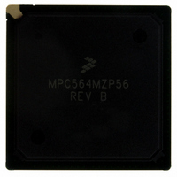
MPC564MZP56 Freescale Semiconductor, MPC564MZP56 Datasheet - Page 427

MPC564MZP56
Manufacturer Part Number
MPC564MZP56
Description
IC MCU 512K FLASH 56MHZ 388-BGA
Manufacturer
Freescale Semiconductor
Series
MPC5xxr
Specifications of MPC564MZP56
Core Processor
PowerPC
Core Size
32-Bit
Speed
56MHz
Connectivity
CAN, EBI/EMI, SCI, SPI, UART/USART
Peripherals
POR, PWM, WDT
Number Of I /o
56
Program Memory Size
512KB (512K x 8)
Program Memory Type
FLASH
Ram Size
32K x 8
Voltage - Supply (vcc/vdd)
2.5 V ~ 2.7 V
Data Converters
A/D 32x10b
Oscillator Type
External
Operating Temperature
-40°C ~ 125°C
Package / Case
388-BGA
Core
PowerPC
Processor Series
MPC5xx
Data Bus Width
32 bit
Maximum Clock Frequency
56 MHz
Data Ram Size
32 KB
On-chip Adc
Yes
Number Of Programmable I/os
56
Number Of Timers
2
Operating Supply Voltage
0 V to 5 V
Mounting Style
SMD/SMT
A/d Bit Size
10 bit
A/d Channels Available
32
Height
1.95 mm
Interface Type
CAN, JTAG, QSPI, SCI, SPI, UART
Length
27 mm
Maximum Operating Temperature
+ 125 C
Minimum Operating Temperature
- 40 C
Supply Voltage (max)
2.7 V, 5.25 V
Supply Voltage (min)
2.5 V, 4.75 V
Width
27 mm
For Use With
MPC564EVB - KIT EVAL FOR MPC561/562/563/564
Lead Free Status / RoHS Status
Contains lead / RoHS non-compliant
Eeprom Size
-
Lead Free Status / Rohs Status
No RoHS Version Available
Available stocks
Company
Part Number
Manufacturer
Quantity
Price
Company:
Part Number:
MPC564MZP56
Manufacturer:
FREESCAL
Quantity:
364
Company:
Part Number:
MPC564MZP56
Manufacturer:
Freescale Semiconductor
Quantity:
10 000
Part Number:
MPC564MZP56
Manufacturer:
FREESCALE
Quantity:
20 000
Company:
Part Number:
MPC564MZP56R2
Manufacturer:
Freescale Semiconductor
Quantity:
10 000
- Current page: 427 of 1420
- Download datasheet (11Mb)
Because it takes two clocks for the external address to be recognized and handled by the memory
controller, the TS which is generated by the external master is ahead of the corresponding CS and strobes
which are asserted by the memory controller. This 2-clock delay might cause problems in some
synchronous memories. To overcome this, the memory controller generates the MTS (memory transfer
start) strobe which can be used in the slave’s memory instead of the external master’s TS signal. As seen
in
the external memory can latch the external master’s address correctly. To activate this feature, the MTSC
bit must be set in the SIUMCR register. Use external logic to control devices that can have burst accesses
from an external master.
On the MPC563, when the external master accesses the internal Flash when it is disabled, the access is
terminated with the transfer error acknowledge (TEA) signal asserted, and the memory controller does not
support this access in any way.
When the memory controller serves an external master, the BDIP signal becomes an input signal. This
signal is watched by the memory controller to detect when the burst is terminated.
Freescale Semiconductor
Figure
NOTE: The memory controller’s BDIP line is used as a burst_in_progress signal.
10-20, the MTS strobe is synchronized to the assertion of CS by the memory controller so that
MPC5xx
Address
BURST
WE/BE
MTS
BDIP
Data
TS
CSx
TA
OE
Configuration for GPCM-Handled Memory Devices
Figure 10-20. Synchronous External Master
TA
MPC561/MPC563 Reference Manual, Rev. 1.2
TS
Synchronous External Master
BDIP
Data
ADDR
BURST
BDIP
BURST
TS
CE
OE
W
Data
Address
Memory
Memory Controller
10-29
Related parts for MPC564MZP56
Image
Part Number
Description
Manufacturer
Datasheet
Request
R

Part Number:
Description:
MPC5 1K0 5%
Manufacturer:
TE Connectivity
Datasheet:

Part Number:
Description:
MPC5 500R 5%
Manufacturer:
TE Connectivity
Datasheet:

Part Number:
Description:
MPC5 5K0 5%
Manufacturer:
Tyco Electronics
Datasheet:

Part Number:
Description:
MPC5 5R0 5%
Manufacturer:
Tyco Electronics
Datasheet:

Part Number:
Description:
MPC5 50K 5%
Manufacturer:
Tyco Electronics
Datasheet:

Part Number:
Description:
MPC5 1R0 5%
Manufacturer:
Tyco Electronics
Datasheet:
Part Number:
Description:
Manufacturer:
Freescale Semiconductor, Inc
Datasheet:
Part Number:
Description:
Manufacturer:
Freescale Semiconductor, Inc
Datasheet:
Part Number:
Description:
Manufacturer:
Freescale Semiconductor, Inc
Datasheet:
Part Number:
Description:
Manufacturer:
Freescale Semiconductor, Inc
Datasheet:
Part Number:
Description:
Manufacturer:
Freescale Semiconductor, Inc
Datasheet:


