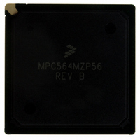
MPC564MZP56 Freescale Semiconductor, MPC564MZP56 Datasheet - Page 114

MPC564MZP56
Manufacturer Part Number
MPC564MZP56
Description
IC MCU 512K FLASH 56MHZ 388-BGA
Manufacturer
Freescale Semiconductor
Series
MPC5xxr
Specifications of MPC564MZP56
Core Processor
PowerPC
Core Size
32-Bit
Speed
56MHz
Connectivity
CAN, EBI/EMI, SCI, SPI, UART/USART
Peripherals
POR, PWM, WDT
Number Of I /o
56
Program Memory Size
512KB (512K x 8)
Program Memory Type
FLASH
Ram Size
32K x 8
Voltage - Supply (vcc/vdd)
2.5 V ~ 2.7 V
Data Converters
A/D 32x10b
Oscillator Type
External
Operating Temperature
-40°C ~ 125°C
Package / Case
388-BGA
Core
PowerPC
Processor Series
MPC5xx
Data Bus Width
32 bit
Maximum Clock Frequency
56 MHz
Data Ram Size
32 KB
On-chip Adc
Yes
Number Of Programmable I/os
56
Number Of Timers
2
Operating Supply Voltage
0 V to 5 V
Mounting Style
SMD/SMT
A/d Bit Size
10 bit
A/d Channels Available
32
Height
1.95 mm
Interface Type
CAN, JTAG, QSPI, SCI, SPI, UART
Length
27 mm
Maximum Operating Temperature
+ 125 C
Minimum Operating Temperature
- 40 C
Supply Voltage (max)
2.7 V, 5.25 V
Supply Voltage (min)
2.5 V, 4.75 V
Width
27 mm
For Use With
MPC564EVB - KIT EVAL FOR MPC561/562/563/564
Lead Free Status / RoHS Status
Contains lead / RoHS non-compliant
Eeprom Size
-
Lead Free Status / Rohs Status
No RoHS Version Available
Available stocks
Company
Part Number
Manufacturer
Quantity
Price
Company:
Part Number:
MPC564MZP56
Manufacturer:
FREESCAL
Quantity:
364
Company:
Part Number:
MPC564MZP56
Manufacturer:
Freescale Semiconductor
Quantity:
10 000
Part Number:
MPC564MZP56
Manufacturer:
FREESCALE
Quantity:
20 000
Company:
Part Number:
MPC564MZP56R2
Manufacturer:
Freescale Semiconductor
Quantity:
10 000
- Current page: 114 of 1420
- Download datasheet (11Mb)
Signal Descriptions
2-16
MPWM1 / MDO2
MPWM2 / PPM_TX1
MPWM3 / PPM_RX1
MPWM16
MPWM17 / MDO3
MPWM[18:19] / MDO[6:7]
Signal Name
Table 2-1. MPC561/MPC563 Signal Descriptions (continued)
Signals
No. of
1
1
1
1
1
2
MPC561/MPC563 Reference Manual, Rev. 1.2
Type
I/O
I/O
I/O
I/O
I/O
I/O
O
O
O
O
I
MPWM1 unless
the Nexus
(READI) port is
enabled, then
MDO2.
See
MPWM2
MPWM3
MPWM16
MPWM17
unless the
Nexus (READI)
port is enabled.
See
MPWM[18:19]
Function after
Section
Section
Reset
1
2.5.
2.5.
Pulse Width Modulation 1. This signal provides a variable
pulse width output signal at a wide range of frequencies.
READI Message Data Out. Message data out (MDO2) is an
output signal used for uploading OTM, BTM, DTM, and
read/write accesses. External latching of MDO occurs on
the rising edge of MCKO. Eight MDO signals are
implemented.
Pulse Width Modulation 2. This signal provides a variable
pulse width output signal at a wide range of frequencies.
PPMTX1. Transmit data from PPM channel number 1.
Pulse Width Modulation 3. This signal provides a variable
pulse width output signal at a wide range of frequencies.
PPMRX1. Receive data to the PPM channel number 1.
Pulse Width Modulation 16. This signal provides a variable
pulse width output at a wide range of frequencies.
Clock Input: MPWM16 can provide a clock input to modulus
clock submodule, MMCSM8
Pulse Width Modulation 17. This signal provides variable
pulse width outputs at a wide range of frequencies.
Load Input: PWM17 can provide a load input to modulus
clock submodule, MMCSM8
READI Message Data Out. Message data out (MDO3) is an
output signal used for uploading OTM, BTM, DTM, and
read/write accesses. External latching of MDO occurs on
rising edge of MCKO. Eight MDO signals are implemented.
Pulse Width Modulation [18:19]. These signals provide
variable pulse width output signals at a wide range of
frequencies.
Clock and Load Input:
READI Message Data Out. Message data out (MDO[6:7])
are output signals used for uploading OTM, BTM, DTM, and
read/write accesses. External latching of MDO occurs on
rising edge of MCKO. Eight MDO signals are implemented.
• MPWM18 can provide clock inputs to modulus counter
• MPWM19 can provide load inputs to modulus counter
submodule MMCSM24
submodule MMCSM24
Description
Freescale Semiconductor
Related parts for MPC564MZP56
Image
Part Number
Description
Manufacturer
Datasheet
Request
R

Part Number:
Description:
MPC5 1K0 5%
Manufacturer:
TE Connectivity
Datasheet:

Part Number:
Description:
MPC5 500R 5%
Manufacturer:
TE Connectivity
Datasheet:

Part Number:
Description:
MPC5 5K0 5%
Manufacturer:
Tyco Electronics
Datasheet:

Part Number:
Description:
MPC5 5R0 5%
Manufacturer:
Tyco Electronics
Datasheet:

Part Number:
Description:
MPC5 50K 5%
Manufacturer:
Tyco Electronics
Datasheet:

Part Number:
Description:
MPC5 1R0 5%
Manufacturer:
Tyco Electronics
Datasheet:
Part Number:
Description:
Manufacturer:
Freescale Semiconductor, Inc
Datasheet:
Part Number:
Description:
Manufacturer:
Freescale Semiconductor, Inc
Datasheet:
Part Number:
Description:
Manufacturer:
Freescale Semiconductor, Inc
Datasheet:
Part Number:
Description:
Manufacturer:
Freescale Semiconductor, Inc
Datasheet:
Part Number:
Description:
Manufacturer:
Freescale Semiconductor, Inc
Datasheet:


