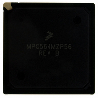
MPC564MZP56 Freescale Semiconductor, MPC564MZP56 Datasheet - Page 856

MPC564MZP56
Manufacturer Part Number
MPC564MZP56
Description
IC MCU 512K FLASH 56MHZ 388-BGA
Manufacturer
Freescale Semiconductor
Series
MPC5xxr
Specifications of MPC564MZP56
Core Processor
PowerPC
Core Size
32-Bit
Speed
56MHz
Connectivity
CAN, EBI/EMI, SCI, SPI, UART/USART
Peripherals
POR, PWM, WDT
Number Of I /o
56
Program Memory Size
512KB (512K x 8)
Program Memory Type
FLASH
Ram Size
32K x 8
Voltage - Supply (vcc/vdd)
2.5 V ~ 2.7 V
Data Converters
A/D 32x10b
Oscillator Type
External
Operating Temperature
-40°C ~ 125°C
Package / Case
388-BGA
Core
PowerPC
Processor Series
MPC5xx
Data Bus Width
32 bit
Maximum Clock Frequency
56 MHz
Data Ram Size
32 KB
On-chip Adc
Yes
Number Of Programmable I/os
56
Number Of Timers
2
Operating Supply Voltage
0 V to 5 V
Mounting Style
SMD/SMT
A/d Bit Size
10 bit
A/d Channels Available
32
Height
1.95 mm
Interface Type
CAN, JTAG, QSPI, SCI, SPI, UART
Length
27 mm
Maximum Operating Temperature
+ 125 C
Minimum Operating Temperature
- 40 C
Supply Voltage (max)
2.7 V, 5.25 V
Supply Voltage (min)
2.5 V, 4.75 V
Width
27 mm
For Use With
MPC564EVB - KIT EVAL FOR MPC561/562/563/564
Lead Free Status / RoHS Status
Contains lead / RoHS non-compliant
Eeprom Size
-
Lead Free Status / Rohs Status
No RoHS Version Available
Available stocks
Company
Part Number
Manufacturer
Quantity
Price
Company:
Part Number:
MPC564MZP56
Manufacturer:
FREESCAL
Quantity:
364
Company:
Part Number:
MPC564MZP56
Manufacturer:
Freescale Semiconductor
Quantity:
10 000
Part Number:
MPC564MZP56
Manufacturer:
FREESCALE
Quantity:
20 000
Company:
Part Number:
MPC564MZP56R2
Manufacturer:
Freescale Semiconductor
Quantity:
10 000
- Current page: 856 of 1420
- Download datasheet (11Mb)
Dual-Port TPU3 RAM (DPTRAM)
20.2
20.3
The DPTRAM module consists of two separately addressable sections. The first is a set of
memory-mapped control and status registers used for configuration (DPTMCR, RAMBAR, MISRH,
MISRL, MISCNT) and testing (DPTTCR) of the DPTRAM array. The second section is the array itself.
All DPTRAM module control and status registers are located in supervisor data space. User read or write
attempts will result in a bus error.
When the TPU3 is using the RAM array for microcode control storage, none of these control registers has
any effect on the operation of the RAM array.
All addresses within the 64-byte control block will respond when accessed properly. Unimplemented
addresses will return zeros for read accesses. Likewise, unimplemented bits within registers will return
zero when read and will not be affected by write operations.
Table 20-1
internal system base address (see
Figure 1-3
20-2
•
•
•
•
— The DPTRAM array acts as a microcode storage for the TPU3 module. This provides a means
Includes built in check logic which scans the array contents and calculates the DPTRAM signature
IMB3 bus interface
Two TPU3 interface units
Byte, half-word, or word accessible
DPTRAM Configuration Block Diagram
Programming Model
to locate the DPTRAM control block in the MPC561/MPC563 address map.
of executing TPU3 code out of DPTRAM instead of TPU3 ROM.
shows the DPTRAM control and status registers. The addresses shown are offsets from the
RAM Mode
DPTRAM
MPC561/MPC563 Reference Manual, Rev. 1.2
TPU3
TPU3
Section 6.2.2.1.2, “Internal Memory Map Register
Figure 20-1. DPTRAM Configuration
TPU3 Emulation Mode
DPTRAM
TPU3
TPU3
Local Bus
Local Bus
Freescale Semiconductor
(IMMR)”). Refer to
Related parts for MPC564MZP56
Image
Part Number
Description
Manufacturer
Datasheet
Request
R

Part Number:
Description:
MPC5 1K0 5%
Manufacturer:
TE Connectivity
Datasheet:

Part Number:
Description:
MPC5 500R 5%
Manufacturer:
TE Connectivity
Datasheet:

Part Number:
Description:
MPC5 5K0 5%
Manufacturer:
Tyco Electronics
Datasheet:

Part Number:
Description:
MPC5 5R0 5%
Manufacturer:
Tyco Electronics
Datasheet:

Part Number:
Description:
MPC5 50K 5%
Manufacturer:
Tyco Electronics
Datasheet:

Part Number:
Description:
MPC5 1R0 5%
Manufacturer:
Tyco Electronics
Datasheet:
Part Number:
Description:
Manufacturer:
Freescale Semiconductor, Inc
Datasheet:
Part Number:
Description:
Manufacturer:
Freescale Semiconductor, Inc
Datasheet:
Part Number:
Description:
Manufacturer:
Freescale Semiconductor, Inc
Datasheet:
Part Number:
Description:
Manufacturer:
Freescale Semiconductor, Inc
Datasheet:
Part Number:
Description:
Manufacturer:
Freescale Semiconductor, Inc
Datasheet:


