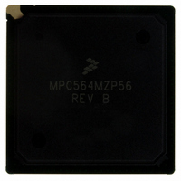
MPC564MZP56 Freescale Semiconductor, MPC564MZP56 Datasheet - Page 629

MPC564MZP56
Manufacturer Part Number
MPC564MZP56
Description
IC MCU 512K FLASH 56MHZ 388-BGA
Manufacturer
Freescale Semiconductor
Series
MPC5xxr
Specifications of MPC564MZP56
Core Processor
PowerPC
Core Size
32-Bit
Speed
56MHz
Connectivity
CAN, EBI/EMI, SCI, SPI, UART/USART
Peripherals
POR, PWM, WDT
Number Of I /o
56
Program Memory Size
512KB (512K x 8)
Program Memory Type
FLASH
Ram Size
32K x 8
Voltage - Supply (vcc/vdd)
2.5 V ~ 2.7 V
Data Converters
A/D 32x10b
Oscillator Type
External
Operating Temperature
-40°C ~ 125°C
Package / Case
388-BGA
Core
PowerPC
Processor Series
MPC5xx
Data Bus Width
32 bit
Maximum Clock Frequency
56 MHz
Data Ram Size
32 KB
On-chip Adc
Yes
Number Of Programmable I/os
56
Number Of Timers
2
Operating Supply Voltage
0 V to 5 V
Mounting Style
SMD/SMT
A/d Bit Size
10 bit
A/d Channels Available
32
Height
1.95 mm
Interface Type
CAN, JTAG, QSPI, SCI, SPI, UART
Length
27 mm
Maximum Operating Temperature
+ 125 C
Minimum Operating Temperature
- 40 C
Supply Voltage (max)
2.7 V, 5.25 V
Supply Voltage (min)
2.5 V, 4.75 V
Width
27 mm
For Use With
MPC564EVB - KIT EVAL FOR MPC561/562/563/564
Lead Free Status / RoHS Status
Contains lead / RoHS non-compliant
Eeprom Size
-
Lead Free Status / Rohs Status
No RoHS Version Available
Available stocks
Company
Part Number
Manufacturer
Quantity
Price
Company:
Part Number:
MPC564MZP56
Manufacturer:
FREESCAL
Quantity:
364
Company:
Part Number:
MPC564MZP56
Manufacturer:
Freescale Semiconductor
Quantity:
10 000
Part Number:
MPC564MZP56
Manufacturer:
FREESCALE
Quantity:
20 000
Company:
Part Number:
MPC564MZP56R2
Manufacturer:
Freescale Semiconductor
Quantity:
10 000
- Current page: 629 of 1420
- Download datasheet (11Mb)
The port QS data register (PORTQS) latches I/O data. PORTQS writes drive pins defined as outputs.
PORTQS reads return data present on the pins. To avoid driving undefined data, write the first data to
PORTQS before configuring DDRQS.
15.5.1
PORTQS determines the actual input or output value of a QSMCM port pin if the pin is defined as
general-purpose input or output. All QSMCM pins can be used as general-purpose input and/or output.
When the SCIx transmitter is disabled, TXDx is a discrete output; when the SCIx receiver is disabled,
RXDx is a discrete input. Writes to this register affect the pins defined as outputs; reads of this register
return the actual value of the pins.
Freescale Semiconductor
Port QS Data Register (PORTQS)
1
QSMCM Pin
The PORTQS register can be written either as a half-word (16-bit) or as 2
individual bytes (8-bit). This allows the SCI GPIO pin data to written
separately than the QSPI GPIO pin values. This allows either the SCI pins
or the QSPI pins to be used independently as GPIO.
PCS0/SS
SCK/QGPIO6 is a digital I/O pin unless the SPI is enabled (SPE set in SPCR1), in which case
it becomes the QSPI serial clock SCK.
PCS[1:3]
MISO
MOSI
SCK
1
Table 15-8. Effect of DDRQS on QSPI Pin Function
Master
Master
Master
Master
Master
Mode
Slave
Slave
Slave
Slave
Slave
MPC561/MPC563 Reference Manual, Rev. 1.2
DDRQS Bit
DDQS[4:6]
DDQS0
DDQS1
DDQS2
DDQS3
NOTE
Bit State
—
—
0
1
0
1
0
1
0
1
0
1
0
1
0
1
0
1
Serial data output from QSPI
Serial data output from QSPI
Assertion causes mode fault
Disables chip-select output
Disables slave select input
Serial data input to QSPI
Serial data input to QSPI
Clock output from QSPI
QSPI slave select input
Disables data output
Disables data output
Clock input to QSPI
Disables data input
Disables data input
Chip-select output
Chip-select output
Pin Function
Inactive
Inactive
Queued Serial Multi-Channel Module
15-11
Related parts for MPC564MZP56
Image
Part Number
Description
Manufacturer
Datasheet
Request
R

Part Number:
Description:
MPC5 1K0 5%
Manufacturer:
TE Connectivity
Datasheet:

Part Number:
Description:
MPC5 500R 5%
Manufacturer:
TE Connectivity
Datasheet:

Part Number:
Description:
MPC5 5K0 5%
Manufacturer:
Tyco Electronics
Datasheet:

Part Number:
Description:
MPC5 5R0 5%
Manufacturer:
Tyco Electronics
Datasheet:

Part Number:
Description:
MPC5 50K 5%
Manufacturer:
Tyco Electronics
Datasheet:

Part Number:
Description:
MPC5 1R0 5%
Manufacturer:
Tyco Electronics
Datasheet:
Part Number:
Description:
Manufacturer:
Freescale Semiconductor, Inc
Datasheet:
Part Number:
Description:
Manufacturer:
Freescale Semiconductor, Inc
Datasheet:
Part Number:
Description:
Manufacturer:
Freescale Semiconductor, Inc
Datasheet:
Part Number:
Description:
Manufacturer:
Freescale Semiconductor, Inc
Datasheet:
Part Number:
Description:
Manufacturer:
Freescale Semiconductor, Inc
Datasheet:


