AC162078 Microchip Technology, AC162078 Datasheet - Page 83
AC162078
Manufacturer Part Number
AC162078
Description
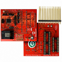
HEADER INTRFC MPLAB ICD2 18F1330
Manufacturer
Microchip Technology
Datasheet
1.AC162078.pdf
(318 pages)
Specifications of AC162078
Accessory Type
Transition Header
Lead Free Status / RoHS Status
Not applicable / Not applicable
For Use With/related Products
ICD2
Lead Free Status / RoHS Status
Lead free / RoHS Compliant, Not applicable / Not applicable
Available stocks
Company
Part Number
Manufacturer
Quantity
Price
Company:

Part Number:
AC162078
Manufacturer:
MICROCHIP
Quantity:
12 000


8.3
To read a data memory location, the user must write the
address to the EEADR register, clear the EEPGD
control bit (EECON1<7>) and then set control bit RD
(EECON1<0>). The data is available for the very next
instruction cycle; therefore, the EEDATA register can
be read by the next instruction. EEDATA will hold this
value until another read operation, or until it is written to
by the user (during a write operation).
8.4
To write an EEPROM data location, the address must
first be written to the EEADR register and the data
written to the EEDATA register. The sequence in
Example 8-2 must be followed to initiate the write cycle.
The write will not begin if this sequence is not exactly
followed (write 55h to EECON2, write 0AAh to
EECON2, then set WR bit) for each byte. It is strongly
recommended that interrupts be disabled during this
code segment.
Additionally, the WREN bit in EECON1 must be set to
enable writes. This mechanism prevents accidental
writes to data EEPROM due to unexpected code
execution (i.e., runaway programs). The WREN bit
should be kept clear at all times, except when updating
the EEPROM. The WREN bit is not cleared
by hardware.
EXAMPLE 8-1:
EXAMPLE 8-2:
2009 Microchip Technology Inc.
Required
Sequence
Reading the Data EEPROM
Memory
Writing to the Data EEPROM
Memory
MOVLW
MOVWF
BCF
BSF
MOVF
MOVLW
MOVWF
MOVLW
MOVWF
BCF
BSF
BCF
MOVLW
MOVWF
MOVLW
MOVWF
BSF
BSF
BTFSC EECON1, WR
BRA $-2
SLEEP
BCF
DATA_EE_ADDR
EEADR
EECON1, EEPGD
EECON1, RD
EEDATA, W
DATA EEPROM READ
DATA EEPROM WRITE
DATA_EE_ADDR
EEADR
DATA_EE_DATA
EEDATA
EECON1, EEPGD
EECON1, WREN
INTCON, GIE
55h
EECON2
0AAh
EECON2
EECON1, WR
INTCON, GIE
EECON1, WREN
;
; Data Memory Address to read
; Point to DATA memory
; EEPROM Read
; W = EEDATA
;
; Data Memory Address to write
;
; Data Memory Value to write
; Point to DATA memory
; Enable writes
; Disable Interrupts
;
; Write 55h
;
; Write 0AAh
; Set WR bit to begin write
; Enable Interrupts
; Wait for write to complete
; Wait for interrupt to signal write complete
; Disable writes
After a write sequence has been initiated, EECON1,
EEADR and EEDATA cannot be modified. The WR bit
will be inhibited from being set unless the WREN bit is
set. The WREN bit must be set on a previous instruc-
tion. Both WR and WREN cannot be set with the same
instruction.
At the completion of the write cycle, the WR bit is
cleared in hardware and the EEPROM Interrupt Flag bit
(EEIF) is set. The user may either enable this interrupt
or poll this bit. EEIF must be cleared by software.
8.5
Depending on the application, good programming
practice may dictate that the value written to the
memory should be verified against the original value.
This should be used in applications where excessive
writes can stress bits near the specification limit.
8.6
There are conditions when the device may not want to
write to the data EEPROM memory. To protect against
spurious EEPROM writes, various mechanisms have
been built-in. On power-up, the WREN bit is cleared.
Also, the Power-up Timer (72 ms duration) prevents
EEPROM write.
The write initiate sequence and the WREN bit together
help prevent an accidental write during brown-out,
power glitch, or software malfunction.
Write Verify
Protection Against Spurious Write
PIC18F1230/1330
DS39758D-page 83
Related parts for AC162078
Image
Part Number
Description
Manufacturer
Datasheet
Request
R

Part Number:
Description:
Manufacturer:
Microchip Technology Inc.
Datasheet:
Part Number:
Description:
Manufacturer:
Microchip Technology Inc.
Datasheet:
Part Number:
Description:
Manufacturer:
Microchip Technology Inc.
Datasheet:
Part Number:
Description:
Manufacturer:
Microchip Technology Inc.
Datasheet:
Part Number:
Description:
Manufacturer:
Microchip Technology Inc.
Datasheet:
Part Number:
Description:
Manufacturer:
Microchip Technology Inc.
Datasheet:
Part Number:
Description:
Manufacturer:
Microchip Technology Inc.
Datasheet:
Part Number:
Description:
Manufacturer:
Microchip Technology Inc.
Datasheet: