AC162078 Microchip Technology, AC162078 Datasheet - Page 131
AC162078
Manufacturer Part Number
AC162078
Description
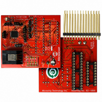
HEADER INTRFC MPLAB ICD2 18F1330
Manufacturer
Microchip Technology
Datasheet
1.AC162078.pdf
(318 pages)
Specifications of AC162078
Accessory Type
Transition Header
Lead Free Status / RoHS Status
Not applicable / Not applicable
For Use With/related Products
ICD2
Lead Free Status / RoHS Status
Lead free / RoHS Compliant, Not applicable / Not applicable
Available stocks
Company
Part Number
Manufacturer
Quantity
Price
Company:

Part Number:
AC162078
Manufacturer:
MICROCHIP
Quantity:
12 000


14.6
PWM duty cycle is defined by the PDCx (PDCxL and
PDCxH) registers. There are a total of three PWM Duty
Cycle registers for four pairs of PWM channels. The
Duty Cycle registers have 14-bit resolution by combin-
ing the six LSbs of PDCxH with the 8 bits of PDCxL.
PDCx is a double-buffered register used to set the
counting period for the PWM time base.
14.6.1
There are three 14-bit Special Function Registers used
to specify duty cycle values for the PWM module:
• PDC0 (PDC0L and PDC0H)
• PDC1 (PDC1L and PDC1H)
• PDC2 (PDC2L and PDC2H)
The value in each Duty Cycle register determines the
amount of time that the PWM output is in the active
state. The upper 12 bits of PDCx hold the actual duty
cycle value from PTMRH/L<11:0>, while the lower two
bits control which internal Q clock the duty cycle match
will occur. This 2-bit value is decoded from the Q
clocks, as shown in Figure 14-11, when the prescaler is
1:1 (PTCKPS<1:0> = 00).
In Edge-Aligned mode, the PWM period starts at Q1 and
ends when the Duty Cycle register matches the PTMR
register as follows. The duty cycle match is considered
when the upper 12 bits of the PDCx are equal to the
FIGURE 14-11:
2009 Microchip Technology Inc.
Note 1: This value is decoded from the Q clocks:
PTMR<11:0>
PDCx<13:0>
PWM Duty Cycle
PWM DUTY CYCLE REGISTERS
00 = duty cycle match occurs on Q1
01 = duty cycle match occurs on Q2
10 = duty cycle match occurs on Q3
11 = duty cycle match occurs on Q4
DUTY CYCLE COMPARISON
Unused
Unused
PTMRH<7:0>
PTMRH<3:0>
PDCxH<7:0>
PDCxH<5:0>
PTMR and the lower 2 bits are equal to Q1, Q2, Q3 or
Q4, depending on the lower two bits of the PDCx (when
the prescaler is 1:1 or PTCKPS<1:0> = 00)
Each compare unit has logic that allows override of the
PWM signals. This logic also ensures that the PWM
signals will complement each other (with dead-time
insertion) in Complementary mode (see Section 14.7
“Dead-Time Generators”).
Note:
Note:
Comparator
PIC18F1230/1330
PTMRL<7:0>
PTMRL<7:0>
When
(PTCKPS<1:0> ~00), the duty cycle
match occurs at the Q1 clock of the
instruction cycle when the PTMR and
PDCx match occurs.
To get the correct PWM duty cycle, always
multiply the calculated PWM duty cycle
value by four before writing it to the PWM
Duty Cycle registers. This is due to the two
additional LSBs in the PWM Duty Cycle
registers which are compared against the
internal Q clock for the PWM duty cycle
match.
the
PDCxL<7:0>
PDCxL<7:0>
prescaler
DS39758D-page 131
is
Q Clocks
.
<1:0>
not
(1)
1:1
Related parts for AC162078
Image
Part Number
Description
Manufacturer
Datasheet
Request
R

Part Number:
Description:
Manufacturer:
Microchip Technology Inc.
Datasheet:
Part Number:
Description:
Manufacturer:
Microchip Technology Inc.
Datasheet:
Part Number:
Description:
Manufacturer:
Microchip Technology Inc.
Datasheet:
Part Number:
Description:
Manufacturer:
Microchip Technology Inc.
Datasheet:
Part Number:
Description:
Manufacturer:
Microchip Technology Inc.
Datasheet:
Part Number:
Description:
Manufacturer:
Microchip Technology Inc.
Datasheet:
Part Number:
Description:
Manufacturer:
Microchip Technology Inc.
Datasheet:
Part Number:
Description:
Manufacturer:
Microchip Technology Inc.
Datasheet: