AC162078 Microchip Technology, AC162078 Datasheet - Page 174
AC162078
Manufacturer Part Number
AC162078
Description
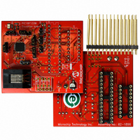
HEADER INTRFC MPLAB ICD2 18F1330
Manufacturer
Microchip Technology
Datasheet
1.AC162078.pdf
(318 pages)
Specifications of AC162078
Accessory Type
Transition Header
Lead Free Status / RoHS Status
Not applicable / Not applicable
For Use With/related Products
ICD2
Lead Free Status / RoHS Status
Lead free / RoHS Compliant, Not applicable / Not applicable
Available stocks
Company
Part Number
Manufacturer
Quantity
Price
Company:

Part Number:
AC162078
Manufacturer:
MICROCHIP
Quantity:
12 000


PIC18F1230/1330
16.1
The A/D conversion can be triggered by setting the GO/
DONE bit. This bit can either be set manually by the
programmer or by setting the SEVTEN bit of ADCON0.
When the SEVTEN bit is set, the Special Event Trigger
from the Power Control PWM module triggers the A/D
conversion. For more information, see Section 14.14
“PWM Special Event Trigger”.
16.2
For the A/D Converter to meet its specified accuracy,
the charge holding capacitor (C
to fully charge to the input channel voltage level. The
analog input model is shown in Figure 16-3. The
source impedance (R
switch (R
required to charge the capacitor C
switch (R
(V
at the analog input (due to pin leakage current). The
maximum recommended impedance for analog
sources is 2.5 k. After the analog input channel is
EQUATION 16-1:
EQUATION 16-2:
EQUATION 16-3:
DS39758D-page 174
T
V
or
T
T
T
T
Temperature coefficient is only required for temperatures > 25C. Below 25C, T
T
T
ACQ
DD
C
ACQ
AMP
COFF
C
ACQ
HOLD
). The source impedance affects the offset voltage
=
=
Triggering A/D Conversions
A/D Acquisition Requirements
SS
=
=
=
=
=
SS
=
=
) impedance varies over the device voltage
Amplifier Settling Time + Holding Capacitor Charging Time + Temperature Coefficient
T
) impedance directly affect the time
AMP
T
0.2 s
(Temp – 25C)(0.02 s/C)
(85C – 25C)(0.02 s/C)
1.2 s
-(C
-(25 pF) (1 k + 2 k + 2.5 k) ln(0.0004883)
1.05 s
0.2 s + 1 s + 1.2 s
2.4 s
(V
-(C
AMP
HOLD
+ T
REF
HOLD
+ T
C
– (V
ACQUISITION TIME
A/D MINIMUM CHARGING TIME
CALCULATING THE MINIMUM REQUIRED ACQUISITION TIME
S
+ T
)(R
C
) and the internal sampling
)(R
+ T
REF
COFF
IC
IC
+ R
COFF
/2048)) • (1 – e
+ R
HOLD
SS
SS
HOLD
+ R
+ R
) must be allowed
S
S
) ln(1/2047)
. The sampling
) ln(1/2048)
(-T
C
/C
HOLD
(R
IC
+ R
SS
+ R
S
selected (changed), the channel must be sampled for
at least the minimum acquisition time before starting a
conversion.
To
Equation 16-1 may be used. This equation assumes
that 1/2 LSb error is used (1024 steps for the A/D). The
1/2 LSb error is the maximum error allowed for the A/D
to meet its specified resolution.
Example 16-3 shows the calculation of the minimum
required acquisition time, T
based
assumptions:
C
Rs
Conversion Error
V
Temperature
))
HOLD
DD
)
Note:
calculate
on
COFF
When the conversion is started, the
holding capacitor is disconnected from the
input pin.
the
= 0 ms.
the
=
=
=
=
following
minimum
2009 Microchip Technology Inc.
25 pF
2.5 k
1/2 LSb
5V R
85C (system max.)
ACQ
SS
. This calculation is
application
acquisition
= 2 k
system
time,
Related parts for AC162078
Image
Part Number
Description
Manufacturer
Datasheet
Request
R

Part Number:
Description:
Manufacturer:
Microchip Technology Inc.
Datasheet:
Part Number:
Description:
Manufacturer:
Microchip Technology Inc.
Datasheet:
Part Number:
Description:
Manufacturer:
Microchip Technology Inc.
Datasheet:
Part Number:
Description:
Manufacturer:
Microchip Technology Inc.
Datasheet:
Part Number:
Description:
Manufacturer:
Microchip Technology Inc.
Datasheet:
Part Number:
Description:
Manufacturer:
Microchip Technology Inc.
Datasheet:
Part Number:
Description:
Manufacturer:
Microchip Technology Inc.
Datasheet:
Part Number:
Description:
Manufacturer:
Microchip Technology Inc.
Datasheet: