AC162078 Microchip Technology, AC162078 Datasheet - Page 191
AC162078
Manufacturer Part Number
AC162078
Description
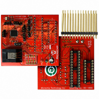
HEADER INTRFC MPLAB ICD2 18F1330
Manufacturer
Microchip Technology
Datasheet
1.AC162078.pdf
(318 pages)
Specifications of AC162078
Accessory Type
Transition Header
Lead Free Status / RoHS Status
Not applicable / Not applicable
For Use With/related Products
ICD2
Lead Free Status / RoHS Status
Lead free / RoHS Compliant, Not applicable / Not applicable
Available stocks
Company
Part Number
Manufacturer
Quantity
Price
Company:

Part Number:
AC162078
Manufacturer:
MICROCHIP
Quantity:
12 000


20.0
PIC18F1230/1330 devices include several features
intended to maximize reliability and minimize cost
through elimination of external components. These
are:
• Oscillator Selection
• Resets:
• Interrupts
• Watchdog Timer (WDT)
• Fail-Safe Clock Monitor
• Two-Speed Start-up
• Code Protection
• ID Locations
• In-Circuit Serial Programming
The oscillator can be configured for the application
depending on frequency, power, accuracy and cost. All
of the options are discussed in detail in Section 3.0
“Oscillator Configurations”.
A complete discussion of device Resets and interrupts
is available in previous sections of this data sheet.
In addition to their Power-up and Oscillator Start-up
Timers provided for Resets, PIC18F1230/1330 devices
have a Watchdog Timer, which is either permanently
enabled via the Configuration bits or software
controlled (if configured as disabled).
TABLE 20-1:
2009 Microchip Technology Inc.
300001h
300002h
300003h
300004h
300005h
300006h
300008h
300009h
30000Ah
30000Bh
30000Ch
30000Dh
3FFFFEh
3FFFFFh
Legend:
Note 1:
- Power-on Reset (POR)
- Power-up Timer (PWRT)
- Oscillator Start-up Timer (OST)
- Brown-out Reset (BOR)
File Name
SPECIAL FEATURES OF
THE CPU
CONFIG1H
CONFIG2L
CONFIG2H
CONFIG3L
CONFIG3H MCLRE
CONFIG4L BKBUG
CONFIG5L
CONFIG5H
CONFIG6L
CONFIG6H WRTD
CONFIG7L
CONFIG7H
DEVID1
DEVID2
- = unimplemented, read as ‘0’.Shaded cells are unimplemented, read as ‘0’.
DEVID registers are read-only and cannot be programmed by the user.
CONFIGURATION BITS AND DEVICE IDs
(1)
(1)
DEV10
DEV2
IESO
Bit 7
CPD
—
—
—
—
—
—
—
FCMEN
EBTRB
XINST
WRTB
DEV1
DEV9
Bit 6
CPB
—
—
—
—
—
—
—
BBSIZ1
WRTC
DEV0
DEV8
Bit 5
—
—
—
—
—
—
—
—
—
—
WDTPS3
BBSIZ0
BORV1
REV4
DEV7
Bit 4
—
—
—
—
—
—
—
—
—
T1OSCMX
WDTPS2
FOSC3
BORV0
DEEV6
HPOL
REV3
The inclusion of an internal RC oscillator also provides
the additional benefits of a Fail-Safe Clock Monitor
(FSCM) and Two-Speed Start-up. FSCM provides for
background monitoring of the peripheral clock and
automatic switchover in the event of its failure. Two-
Speed Start-up enables code to be executed almost
immediately on start-up while the primary clock source
completes its start-up delays.
All of these features are enabled and configured by
setting the appropriate Configuration register bits.
20.1
The Configuration bits can be programmed (read as
‘0’) or left unprogrammed (read as ‘1’) to select various
device configurations. These bits are mapped starting
at program memory location 300000h.
The user will note that address 300000h is beyond the
user program memory space. In fact, it belongs to the
configuration memory space (300000h-3FFFFFh) which
can only be accessed using table reads and table writes.
Programming the Configuration registers is done in a
manner similar to programming the Flash memory. The
WR bit in the EECON1 register starts a self-timed write
to the Configuration register. In normal operation
mode, a TBLWT instruction with the TBLPTR pointing to
the Configuration register sets up the address and data
for the Configuration register write. Setting the WR bit
starts a long write to the Configuration register. The
Configuration registers are written a byte at a time. To
write or erase a configuration cell, a TBLWT instruction
can write a ‘1’ or a ‘0’ into the cell. For additional details
on Flash programming, refer to Section 7.5 “Writing
to Flash Program Memory”.
Bit 3
—
—
—
—
—
—
—
Configuration Bits
WDTPS1 WDTPS0 WDTEN
PIC18F1230/1330
BOREN1 BOREN0 PWRTEN
FOSC2
LPOL
REV2
DEV5
Bit 2
—
—
—
—
—
—
—
—
PWMPIN
FOSC1
EBTR1
WRT1
REV1
DEV4
Bit 1
CP1
—
—
—
—
—
STVREN
FLTAMX
FOSC0
EBTR0
WRT0
REV0
DEV3
Bit 0
CP0
—
—
—
—
DS39758D-page 191
Unprogrammed
See Table 20-2
See Table 20-2
00-- 0111
---1 1111
---1 1111
---- 111-
1--- 0--1
1000 ---1
---- --11
11-- ----
---- --11
111- ----
---- --11
-1-- ----
Default/
Value
Related parts for AC162078
Image
Part Number
Description
Manufacturer
Datasheet
Request
R

Part Number:
Description:
Manufacturer:
Microchip Technology Inc.
Datasheet:
Part Number:
Description:
Manufacturer:
Microchip Technology Inc.
Datasheet:
Part Number:
Description:
Manufacturer:
Microchip Technology Inc.
Datasheet:
Part Number:
Description:
Manufacturer:
Microchip Technology Inc.
Datasheet:
Part Number:
Description:
Manufacturer:
Microchip Technology Inc.
Datasheet:
Part Number:
Description:
Manufacturer:
Microchip Technology Inc.
Datasheet:
Part Number:
Description:
Manufacturer:
Microchip Technology Inc.
Datasheet:
Part Number:
Description:
Manufacturer:
Microchip Technology Inc.
Datasheet: