AC162078 Microchip Technology, AC162078 Datasheet - Page 81
AC162078
Manufacturer Part Number
AC162078
Description
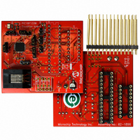
HEADER INTRFC MPLAB ICD2 18F1330
Manufacturer
Microchip Technology
Datasheet
1.AC162078.pdf
(318 pages)
Specifications of AC162078
Accessory Type
Transition Header
Lead Free Status / RoHS Status
Not applicable / Not applicable
For Use With/related Products
ICD2
Lead Free Status / RoHS Status
Lead free / RoHS Compliant, Not applicable / Not applicable
Available stocks
Company
Part Number
Manufacturer
Quantity
Price
Company:

Part Number:
AC162078
Manufacturer:
MICROCHIP
Quantity:
12 000


8.0
The data EEPROM is readable and writable during
normal operation over the entire V
memory is not directly mapped in the register file
space. Instead, it is indirectly addressed through the
Special Function Registers (SFR).
There are four SFRs used to read and write the
program and data EEPROM memory. These registers
are:
• EECON1
• EECON2
• EEDATA
• EEADR
The EEPROM data memory allows byte read and write.
When interfacing to the data memory block, EEDATA
holds the 8-bit data for read/write and EEADR holds the
address of the EEPROM location being accessed.
These devices have 128 bytes of data EEPROM with
an address range from 00h to FFh.
The EEPROM data memory is rated for high erase/
write cycle endurance. A byte write automatically
erases the location and writes the new data (erase-
before-write). The write time is controlled by an on-chip
timer. The write time will vary with voltage and
temperature, as well as from chip-to-chip. Please
refer to parameter D122 (Table in Section 23.0
“Electrical Characteristics”) for exact limits.
8.1
The EEPROM Address register can address 256 bytes
of data EEPROM.
2009 Microchip Technology Inc.
DATA EEPROM MEMORY
EEADR Register
DD
range. The data
8.2
Access to the data EEPROM is controlled by two
registers: EECON1 and EECON2. These are the same
registers which control access to the program memory
and are used in a similar manner for the data
EEPROM.
The EECON1 register (Register 7-1) is the control reg-
ister for data and program memory access. Control bit
EEPGD determines if the access will be to program or
data EEPROM memory. When clear, operations will
access the data EEPROM memory. When set, program
memory is accessed.
Control bit, CFGS, determines if the access will be to
the Configuration registers or to program memory/data
EEPROM memory. When set, subsequent operations
access Configuration registers. When CFGS is clear,
the EEPGD bit selects either program Flash or data
EEPROM memory.
The WREN bit, when set, will allow a write operation.
On power-up, the WREN bit is clear. The WRERR bit is
set in hardware when the WREN bit is set and cleared
when the internal programming timer expires and the
write operation is complete.
The RD bit cannot be set when accessing program
memory (EEPGD = 1). Program memory is read using
table read instructions. See Section 7.1 “Table Reads
and Table Writes” regarding table reads.
Note:
Note 1: During normal operation, the WRERR bit
2: The Interrupt Flag bit, EEIF in the PIR2
EECON1 and EECON2 Registers
PIC18F1230/1330
The EECON2 register is not a physical
register. It is used exclusively in the mem-
ory write and erase sequences. Reading
EECON2 will read all ‘0’s.
is read as ‘1’. This can indicate that a
write operation was prematurely termi-
nated by a Reset, or a write operation
was attempted improperly. The WR con-
trol bit initiates write operations. The bit
cannot be cleared, only set, in software; it
is cleared in hardware at the completion
of the write operation.
register, is set when write is complete. It
must be cleared in the software Control
bits RD and WR, start read and erase/
write operations, respectively. These bits
are set by firmware and cleared by
hardware at the completion of the
operation.
DS39758D-page 81
Related parts for AC162078
Image
Part Number
Description
Manufacturer
Datasheet
Request
R

Part Number:
Description:
Manufacturer:
Microchip Technology Inc.
Datasheet:
Part Number:
Description:
Manufacturer:
Microchip Technology Inc.
Datasheet:
Part Number:
Description:
Manufacturer:
Microchip Technology Inc.
Datasheet:
Part Number:
Description:
Manufacturer:
Microchip Technology Inc.
Datasheet:
Part Number:
Description:
Manufacturer:
Microchip Technology Inc.
Datasheet:
Part Number:
Description:
Manufacturer:
Microchip Technology Inc.
Datasheet:
Part Number:
Description:
Manufacturer:
Microchip Technology Inc.
Datasheet:
Part Number:
Description:
Manufacturer:
Microchip Technology Inc.
Datasheet: