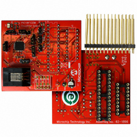
AC162078 Microchip Technology, AC162078 Datasheet - Page 29

AC162078
Manufacturer Part Number
AC162078
Description
HEADER INTRFC MPLAB ICD2 18F1330
Manufacturer
Microchip Technology
Datasheet
1.AC162078.pdf
(318 pages)
Specifications of AC162078
Accessory Type
Transition Header
Lead Free Status / RoHS Status
Not applicable / Not applicable
For Use With/related Products
ICD2
Lead Free Status / RoHS Status
Lead free / RoHS Compliant, Not applicable / Not applicable
Available stocks
Company
Part Number
Manufacturer
Quantity
Price
Company:
Part Number:
AC162078
Manufacturer:
MICROCHIP
Quantity:
12 000
- Current page: 29 of 318
- Download datasheet (3Mb)
3.8
When PRI_IDLE mode is selected, the designated
primary oscillator continues to run without interruption.
For all other power-managed modes, the oscillator
using the OSC1 pin is disabled. The OSC1 pin (and
OSC2 pin, if used by the oscillator) will stop oscillating.
In
SEC_IDLE), the Timer1 oscillator is operating and
providing the device clock. The Timer1 oscillator may
also run in all power-managed modes if required to
clock Timer1 or Timer3.
In internal oscillator modes (RC_RUN and RC_IDLE),
the internal oscillator block provides the device clock
source. The 31 kHz INTRC output can be used directly
to provide the clock and may be enabled to support
various special features, regardless of the power-
managed mode (see Section 20.2 “Watchdog Timer
(WDT)”, Section 20.3 “Two-Speed Start-up” and
Section 20.4 “Fail-Safe Clock Monitor” for more
information on WDT, Fail-Safe Clock Monitor and Two-
Speed Start-up). The INTOSC output at 8 MHz may be
used directly to clock the device or may be divided
down by the postscaler. The INTOSC output is disabled
if the clock is provided directly from the INTRC output.
If the Sleep mode is selected, all clock sources are
stopped. Since all the transistor switching currents
have been stopped, Sleep mode achieves the lowest
current consumption of the device (only leakage
currents).
Enabling any on-chip feature that will operate during
Sleep will increase the current consumed during Sleep.
The INTRC is required to support WDT operation. The
Timer1 oscillator may be operating to support a real-
TABLE 3-3:
2009 Microchip Technology Inc.
RC, INTIO1
RCIO
INTIO2
ECIO
EC
LP, XT and HS
Note:
secondary
Oscillator Mode
Effects of Power-Managed Modes
on the Various Clock Sources
See Table 5-2 in Section 5.0 “Reset” for time-outs due to Sleep and MCLR Reset.
OSC1 AND OSC2 PIN STATES IN SLEEP MODE
clock
modes
Floating, external resistor should pull high
Floating, external resistor should pull high
Configured as PORTA, bit 7
Floating, pulled by external clock
Floating, pulled by external clock
Feedback inverter disabled at quiescent
voltage level
(SEC_RUN
OSC1 Pin
and
time clock. Other features may be operating that do not
require a device clock source (i.e., INTx pins and
others). Peripherals that may add significant current
consumption are listed in Section 23.0 “Electrical
Characteristics”.
3.9
Power-up delays are controlled by two timers, so that no
external Reset circuitry is required for most applications.
The delays ensure that the device is kept in Reset until
the device power supply is stable under normal
circumstances and the primary clock is operating and
stable. For additional information on power-up delays,
see Section 5.5 “Device Reset Timers”.
The first timer is the Power-up Timer (PWRT), which
provides a fixed delay on power-up (parameter 33,
Table 23-10). It is enabled by clearing (= 0) the
PWRTEN Configuration bit.
The second timer is the Oscillator Start-up Timer
(OST), intended to keep the chip in Reset until the
crystal oscillator is stable (LP, XT and HS modes). The
OST does this by counting 1024 oscillator cycles
before allowing the oscillator to clock the device.
When the HSPLL Oscillator mode is selected, the
device is kept in Reset for an additional 2 ms, following
the HS mode OST delay, so the PLL can lock to the
incoming clock frequency.
There is a delay of interval T
Table 23-10), following POR, while the controller
becomes ready to execute instructions. This delay runs
concurrently with any other delays. This may be the
only delay that occurs when any of the EC, RC or INTIO
modes are used as the primary clock source.
Power-up Delays
PIC18F1230/1330
At logic low (clock/4 output)
Configured as PORTA, bit 6
Configured as PORTA, bit 6
Configured as PORTA, bit 6
At logic low (clock/4 output)
Feedback inverter disabled at quiescent
voltage level
OSC2 Pin
CSD
DS39758D-page 29
(parameter 38,
Related parts for AC162078
Image
Part Number
Description
Manufacturer
Datasheet
Request
R

Part Number:
Description:
Manufacturer:
Microchip Technology Inc.
Datasheet:

Part Number:
Description:
Manufacturer:
Microchip Technology Inc.
Datasheet:

Part Number:
Description:
Manufacturer:
Microchip Technology Inc.
Datasheet:

Part Number:
Description:
Manufacturer:
Microchip Technology Inc.
Datasheet:

Part Number:
Description:
Manufacturer:
Microchip Technology Inc.
Datasheet:

Part Number:
Description:
Manufacturer:
Microchip Technology Inc.
Datasheet:

Part Number:
Description:
Manufacturer:
Microchip Technology Inc.
Datasheet:

Part Number:
Description:
Manufacturer:
Microchip Technology Inc.
Datasheet:


