AC162078 Microchip Technology, AC162078 Datasheet - Page 169
AC162078
Manufacturer Part Number
AC162078
Description
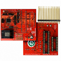
HEADER INTRFC MPLAB ICD2 18F1330
Manufacturer
Microchip Technology
Datasheet
1.AC162078.pdf
(318 pages)
Specifications of AC162078
Accessory Type
Transition Header
Lead Free Status / RoHS Status
Not applicable / Not applicable
For Use With/related Products
ICD2
Lead Free Status / RoHS Status
Lead free / RoHS Compliant, Not applicable / Not applicable
Available stocks
Company
Part Number
Manufacturer
Quantity
Price
Company:

Part Number:
AC162078
Manufacturer:
MICROCHIP
Quantity:
12 000


16.0
The Analog-to-Digital (A/D) Converter module has
4 inputs for the 18/20/28-pin devices. This module
allows conversion of an analog input signal to a
corresponding 10-bit digital number in PIC18F1230/
1330 devices.
The module has five registers:
• A/D Result Register High Byte (ADRESH)
• A/D Result Register Low Byte (ADRESL)
• A/D Control Register 0 (ADCON0)
• A/D Control Register 1 (ADCON1)
• A/D Control Register 2 (ADCON2)
REGISTER 16-1:
2009 Microchip Technology Inc.
bit 7
Legend:
R = Readable bit
-n = Value at POR
bit 7
bit 6-4
bit 3-2
bit 1
bit 0
SEVTEN
R/W-0
10-BIT ANALOG-TO-DIGITAL
CONVERTER (A/D) MODULE
SEVTEN: Special Event Trigger Enable bit
1 = Special Event Trigger from Power Control PWM module is enabled
0 = Special Event Trigger from Power Control PWM module is disabled (default)
Unimplemented: Read as ‘0’
CHS1:CHS0: Analog Channel Select bits
00 = Channel 0 (AN0)
01 = Channel 1 (AN1)
10 = Channel 2 (AN2)
11 = Channel 3 (AN3)
GO/DONE: A/D Conversion Status bit
When ADON = 1:
1 = A/D conversion in progress
0 = A/D Idle
ADON: A/D On bit
1 = A/D Converter module is enabled
0 = A/D Converter module is disabled
U-0
—
ADCON0: A/D CONTROL REGISTER 0
W = Writable bit
‘1’ = Bit is set
U-0
—
U-0
—
U = Unimplemented bit, read as ‘0’
‘0’ = Bit is cleared
R/W-0
CHS1
The ADCON0 register, shown in Register 16-1,
controls the operation of the A/D module. The
ADCON1 register, shown in Register 16-2, configures
the functions of the port pins. The ADCON2 register,
shown in Register 16-3, configures the A/D clock
source, programmed acquisition time and justification.
PIC18F1230/1330
R/W-0
CHS0
x = Bit is unknown
GO/DONE
R/W-0
DS39758D-page 169
R/W-0
ADON
bit 0
Related parts for AC162078
Image
Part Number
Description
Manufacturer
Datasheet
Request
R

Part Number:
Description:
Manufacturer:
Microchip Technology Inc.
Datasheet:
Part Number:
Description:
Manufacturer:
Microchip Technology Inc.
Datasheet:
Part Number:
Description:
Manufacturer:
Microchip Technology Inc.
Datasheet:
Part Number:
Description:
Manufacturer:
Microchip Technology Inc.
Datasheet:
Part Number:
Description:
Manufacturer:
Microchip Technology Inc.
Datasheet:
Part Number:
Description:
Manufacturer:
Microchip Technology Inc.
Datasheet:
Part Number:
Description:
Manufacturer:
Microchip Technology Inc.
Datasheet:
Part Number:
Description:
Manufacturer:
Microchip Technology Inc.
Datasheet: