AC162078 Microchip Technology, AC162078 Datasheet - Page 173
AC162078
Manufacturer Part Number
AC162078
Description
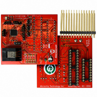
HEADER INTRFC MPLAB ICD2 18F1330
Manufacturer
Microchip Technology
Datasheet
1.AC162078.pdf
(318 pages)
Specifications of AC162078
Accessory Type
Transition Header
Lead Free Status / RoHS Status
Not applicable / Not applicable
For Use With/related Products
ICD2
Lead Free Status / RoHS Status
Lead free / RoHS Compliant, Not applicable / Not applicable
Available stocks
Company
Part Number
Manufacturer
Quantity
Price
Company:

Part Number:
AC162078
Manufacturer:
MICROCHIP
Quantity:
12 000


The value in the ADRESH:ADRESL registers is not
modified for a Power-on Reset. The ADRESH:ADRESL
registers will contain unknown data after a Power-on
Reset.
After the A/D module has been configured as desired,
the selected channel must be acquired before the
conversion is started. The analog input channels must
have their corresponding TRIS bits selected as inputs.
To determine acquisition time, see Section 16.2 “A/D
Acquisition Requirements”. After this acquisition
time has elapsed, the A/D conversion can be started.
An acquisition time can be programmed to occur
between setting the GO/DONE bit and the actual start
of the conversion.
The following steps should be followed to perform an A/
D conversion:
1.
2.
3.
4.
FIGURE 16-3:
2009 Microchip Technology Inc.
Configure the A/D module:
• Configure analog pins, voltage reference and
• Select A/D input channel (ADCON0)
• Select A/D acquisition time (ADCON2)
• Select A/D conversion clock (ADCON2)
• Turn on A/D module (ADCON0)
Configure A/D interrupt (if desired):
• Clear ADIF bit
• Set ADIE bit
• Set GIE bit
Wait the required acquisition time (if required).
Start conversion:
• Set GO/DONE bit (ADCON0 register)
digital I/O (ADCON1)
Legend: C
V
AIN
Rs
V
I
R
SS
C
R
LEAKAGE
PIN
T
IC
HOLD
SS
ANALOG INPUT MODEL
ANx
C
5 pF
PIN
= Input Capacitance
= Threshold Voltage
= Leakage Current at the pin due to
= Interconnect Resistance
= Sampling Switch
= Sample/Hold Capacitance (from DAC)
= Sampling Switch Resistance
various junctions
V
DD
V
V
T
T
= 0.6V
= 0.6V
I
±100 nA
5.
6.
7.
FIGURE 16-2:
LEAKAGE
R
Wait for A/D conversion to complete, by either:
• Polling for the GO/DONE bit to be cleared
OR
• Waiting for the A/D interrupt
Read A/D Result registers (ADRESH:ADRESL);
clear bit ADIF, if required.
For next conversion, go to step 1 or step 2, as
required. The A/D conversion time per bit is
defined as T
required before the next acquisition starts.
IC
3FEh
3FFh
003h
002h
001h
000h
1k
PIC18F1230/1330
V
DD
SS
Sampling
Switch
AD
6V
5V
4V
3V
2V
R
. A minimum wait of 2 T
SS
A/D TRANSFER FUNCTION
Analog Input Voltage
Sampling Switch (k)
1
C
V
2
SS
HOLD
3
DS39758D-page 173
= 25 pF
4
AD
is
Related parts for AC162078
Image
Part Number
Description
Manufacturer
Datasheet
Request
R

Part Number:
Description:
Manufacturer:
Microchip Technology Inc.
Datasheet:
Part Number:
Description:
Manufacturer:
Microchip Technology Inc.
Datasheet:
Part Number:
Description:
Manufacturer:
Microchip Technology Inc.
Datasheet:
Part Number:
Description:
Manufacturer:
Microchip Technology Inc.
Datasheet:
Part Number:
Description:
Manufacturer:
Microchip Technology Inc.
Datasheet:
Part Number:
Description:
Manufacturer:
Microchip Technology Inc.
Datasheet:
Part Number:
Description:
Manufacturer:
Microchip Technology Inc.
Datasheet:
Part Number:
Description:
Manufacturer:
Microchip Technology Inc.
Datasheet: