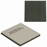
EP3SL150F1152C2N Altera, EP3SL150F1152C2N Datasheet - Page 400

EP3SL150F1152C2N
Manufacturer Part Number
EP3SL150F1152C2N
Description
IC STRATX III FPGA 150K 1152FBGA
Manufacturer
Altera
Series
Stratix® IIIr
Datasheets
1.EP3SL150F780C4N.pdf
(16 pages)
2.EP3SL150F780C4N.pdf
(332 pages)
3.EP3SL150F780C4N.pdf
(456 pages)
Specifications of EP3SL150F1152C2N
Number Of Logic Elements/cells
142500
Number Of Labs/clbs
5700
Total Ram Bits
6390
Number Of I /o
744
Voltage - Supply
0.86 V ~ 1.15 V
Mounting Type
Surface Mount
Operating Temperature
0°C ~ 85°C
Package / Case
1152-FBGA
For Use With
544-2568 - KIT DEVELOPMENT STRATIX III
Lead Free Status / RoHS Status
Lead free / RoHS Compliant
Number Of Gates
-
Other names
544-2409
EP3SL150F1152C2NES
EP3SL150F1152C2NES
Available stocks
Company
Part Number
Manufacturer
Quantity
Price
Part Number:
EP3SL150F1152C2N
Manufacturer:
ALTERA
Quantity:
20 000
- Current page: 400 of 456
- Download datasheet (7Mb)
13–2
Table 13–1. IEEE Std. 1149.1 Pin Descriptions
Stratix III Device Handbook, Volume 1
TDI
TDO
TMS
TCK
TRST
Note to
(1) The minimum TRST pulse width to reset the JTAG TAP controller is 60 ns.
Pin
Table
(1)
13–1:
Test data input
Test data output
Test mode select
Test clock input
Test reset input
(optional)
Description
Table 13–1
The IEEE Std. 1149.1 BST circuitry requires the following registers:
■
■
■
The instruction register determines the action to be performed and the data
register to be accessed.
The bypass register is a one-bit-long data register that provides a minimum-length
serial path between TDI and TDO.
The boundary-scan register is a shift register composed of all the boundary-scan
cells of the device.
summarizes the functions of each of these pins.
Serial input pin for instructions as well as test and programming data. Signal applied
to TDI is expected to change state at the falling edge of TCK. Data is shifted in on
the rising edge of TCK.
Serial data output pin for instructions as well as test and programming data. Data is
shifted out on the falling edge of TCK. The pin is tri-stated if data is not being shifted
out of the device.
Input pin that provides the control signal to determine the transitions of the test
access port (TAP) controller state machine. Transitions within the state machine
occur at the rising edge of TCK. Therefore, you must set up TMS before the rising
edge of TCK. TMS is evaluated on the rising edge of TCK. During non-JTAG
operation, Altera recommends you drive TMS high.
The clock input to the BST circuitry. Some operations occur at the rising edge, while
others occur at the falling edge.
Active-low input to asynchronously reset the boundary-scan circuit. For non-JTAG
users, you should permanently tie the pin to GND.
Chapter 13: IEEE 1149.1 (JTAG) Boundary-Scan Testing in Stratix III Devices
Function
IEEE Std. 1149.1 BST Architecture
© July 2010 Altera Corporation
Related parts for EP3SL150F1152C2N
Image
Part Number
Description
Manufacturer
Datasheet
Request
R

Part Number:
Description:
CYCLONE II STARTER KIT EP2C20N
Manufacturer:
Altera
Datasheet:

Part Number:
Description:
CPLD, EP610 Family, ECMOS Process, 300 Gates, 16 Macro Cells, 16 Reg., 16 User I/Os, 5V Supply, 35 Speed Grade, 24DIP
Manufacturer:
Altera Corporation
Datasheet:

Part Number:
Description:
CPLD, EP610 Family, ECMOS Process, 300 Gates, 16 Macro Cells, 16 Reg., 16 User I/Os, 5V Supply, 15 Speed Grade, 24DIP
Manufacturer:
Altera Corporation
Datasheet:

Part Number:
Description:
Manufacturer:
Altera Corporation
Datasheet:

Part Number:
Description:
CPLD, EP610 Family, ECMOS Process, 300 Gates, 16 Macro Cells, 16 Reg., 16 User I/Os, 5V Supply, 30 Speed Grade, 24DIP
Manufacturer:
Altera Corporation
Datasheet:

Part Number:
Description:
High-performance, low-power erasable programmable logic devices with 8 macrocells, 10ns
Manufacturer:
Altera Corporation
Datasheet:

Part Number:
Description:
High-performance, low-power erasable programmable logic devices with 8 macrocells, 7ns
Manufacturer:
Altera Corporation
Datasheet:

Part Number:
Description:
Classic EPLD
Manufacturer:
Altera Corporation
Datasheet:

Part Number:
Description:
High-performance, low-power erasable programmable logic devices with 8 macrocells, 10ns
Manufacturer:
Altera Corporation
Datasheet:

Part Number:
Description:
Manufacturer:
Altera Corporation
Datasheet:

Part Number:
Description:
Manufacturer:
Altera Corporation
Datasheet:

Part Number:
Description:
Manufacturer:
Altera Corporation
Datasheet:

Part Number:
Description:
CPLD, EP610 Family, ECMOS Process, 300 Gates, 16 Macro Cells, 16 Reg., 16 User I/Os, 5V Supply, 25 Speed Grade, 24DIP
Manufacturer:
Altera Corporation
Datasheet:


