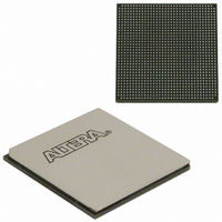
EP3SL150F1152C2N Altera, EP3SL150F1152C2N Datasheet - Page 309

EP3SL150F1152C2N
Manufacturer Part Number
EP3SL150F1152C2N
Description
IC STRATX III FPGA 150K 1152FBGA
Manufacturer
Altera
Series
Stratix® IIIr
Datasheets
1.EP3SL150F780C4N.pdf
(16 pages)
2.EP3SL150F780C4N.pdf
(332 pages)
3.EP3SL150F780C4N.pdf
(456 pages)
Specifications of EP3SL150F1152C2N
Number Of Logic Elements/cells
142500
Number Of Labs/clbs
5700
Total Ram Bits
6390
Number Of I /o
744
Voltage - Supply
0.86 V ~ 1.15 V
Mounting Type
Surface Mount
Operating Temperature
0°C ~ 85°C
Package / Case
1152-FBGA
For Use With
544-2568 - KIT DEVELOPMENT STRATIX III
Lead Free Status / RoHS Status
Lead free / RoHS Compliant
Number Of Gates
-
Other names
544-2409
EP3SL150F1152C2NES
EP3SL150F1152C2NES
Available stocks
Company
Part Number
Manufacturer
Quantity
Price
Part Number:
EP3SL150F1152C2N
Manufacturer:
ALTERA
Quantity:
20 000
- Current page: 309 of 456
- Download datasheet (7Mb)
Chapter 9: High-Speed Differential I/O Interfaces and DPA in Stratix III Devices
Clocking
Source-Synchronous Timing Budget
Differential Data Orientation
Figure 9–15. Bit Orientation in Quartus II Software
Differential I/O Bit Position
© July 2010
Altera Corporation
inclock/outclock
This section discusses the timing budget, waveforms, and specifications for
source-synchronous signaling in Stratix III devices. LVDS I/O standards enable
high-speed data transmission. This high data transmission rate results in better
overall system performance. To take advantage of fast system performance, it is
important to understand how to analyze timing for these high-speed signals. Timing
analysis for the differential block is different from traditional synchronous timing
analysis techniques.
Rather than focusing on clock-to-output and setup times, source synchronous timing
analysis is based on the skew between the data and the clock signals. High-speed
differential data transmission requires the use of timing parameters provided by IC
vendors and is strongly influenced by board skew, cable skew, and clock jitter. This
section defines the source-synchronous differential data orientation timing
parameters, the timing budget definitions for Stratix III devices, and ways to use these
timing parameters to determine the maximum performance of your design.
There is a set relationship between an external clock and the incoming data. For an
operation at 1 Gbps and SERDES factor of 10, the external clock is multiplied by 10,
and phase-alignment can be set in the PLL to coincide with the sampling window of
each data bit. The data is sampled on the falling edge of the multiplied clock.
Figure 9–15
Data synchronization is necessary for successful data transmission at high
frequencies.
figures are based on the following:
■
■
■
For other serialization factors, use the Quartus II software tools and find the bit
position within the word and the bit positions after deserialization.
SERDES factor equals clock multiplication factor
Edge alignment is selected for phase alignment
Implemented in hard SERDES
data in
shows the data bit orientation of the ×10 mode.
Figure 9–16
MSB
9
shows the data bit orientation for a channel operation. These
8
7
6
10 LVDS Bits
5
4
3
2
1
Stratix III Device Handbook, Volume 1
LSB
0
9–15
Related parts for EP3SL150F1152C2N
Image
Part Number
Description
Manufacturer
Datasheet
Request
R

Part Number:
Description:
CYCLONE II STARTER KIT EP2C20N
Manufacturer:
Altera
Datasheet:

Part Number:
Description:
CPLD, EP610 Family, ECMOS Process, 300 Gates, 16 Macro Cells, 16 Reg., 16 User I/Os, 5V Supply, 35 Speed Grade, 24DIP
Manufacturer:
Altera Corporation
Datasheet:

Part Number:
Description:
CPLD, EP610 Family, ECMOS Process, 300 Gates, 16 Macro Cells, 16 Reg., 16 User I/Os, 5V Supply, 15 Speed Grade, 24DIP
Manufacturer:
Altera Corporation
Datasheet:

Part Number:
Description:
Manufacturer:
Altera Corporation
Datasheet:

Part Number:
Description:
CPLD, EP610 Family, ECMOS Process, 300 Gates, 16 Macro Cells, 16 Reg., 16 User I/Os, 5V Supply, 30 Speed Grade, 24DIP
Manufacturer:
Altera Corporation
Datasheet:

Part Number:
Description:
High-performance, low-power erasable programmable logic devices with 8 macrocells, 10ns
Manufacturer:
Altera Corporation
Datasheet:

Part Number:
Description:
High-performance, low-power erasable programmable logic devices with 8 macrocells, 7ns
Manufacturer:
Altera Corporation
Datasheet:

Part Number:
Description:
Classic EPLD
Manufacturer:
Altera Corporation
Datasheet:

Part Number:
Description:
High-performance, low-power erasable programmable logic devices with 8 macrocells, 10ns
Manufacturer:
Altera Corporation
Datasheet:

Part Number:
Description:
Manufacturer:
Altera Corporation
Datasheet:

Part Number:
Description:
Manufacturer:
Altera Corporation
Datasheet:

Part Number:
Description:
Manufacturer:
Altera Corporation
Datasheet:

Part Number:
Description:
CPLD, EP610 Family, ECMOS Process, 300 Gates, 16 Macro Cells, 16 Reg., 16 User I/Os, 5V Supply, 25 Speed Grade, 24DIP
Manufacturer:
Altera Corporation
Datasheet:


