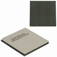
EP3SL150F1152C2N Altera, EP3SL150F1152C2N Datasheet - Page 177

EP3SL150F1152C2N
Manufacturer Part Number
EP3SL150F1152C2N
Description
IC STRATX III FPGA 150K 1152FBGA
Manufacturer
Altera
Series
Stratix® IIIr
Datasheets
1.EP3SL150F780C4N.pdf
(16 pages)
2.EP3SL150F780C4N.pdf
(332 pages)
3.EP3SL150F780C4N.pdf
(456 pages)
Specifications of EP3SL150F1152C2N
Number Of Logic Elements/cells
142500
Number Of Labs/clbs
5700
Total Ram Bits
6390
Number Of I /o
744
Voltage - Supply
0.86 V ~ 1.15 V
Mounting Type
Surface Mount
Operating Temperature
0°C ~ 85°C
Package / Case
1152-FBGA
For Use With
544-2568 - KIT DEVELOPMENT STRATIX III
Lead Free Status / RoHS Status
Lead free / RoHS Compliant
Number Of Gates
-
Other names
544-2409
EP3SL150F1152C2NES
EP3SL150F1152C2NES
Available stocks
Company
Part Number
Manufacturer
Quantity
Price
Part Number:
EP3SL150F1152C2N
Manufacturer:
ALTERA
Quantity:
20 000
- Current page: 177 of 456
- Download datasheet (7Mb)
Chapter 6: Clock Networks and PLLs in Stratix III Devices
PLLs in Stratix III Devices
Figure 6–27. Zero-Delay Buffer Mode in Stratix III PLLs
© July 2010
Altera Corporation
1
1
inclk
Figure 6–26. Phase Relationship Between PLL Clocks in Normal Mode
Note to
(1) The external clock output can lead or lag the PLL internal clock signals.
Zero-Delay Buffer Mode
In zero-delay buffer (ZDB) mode, the external clock output pin is phase-aligned with
the clock input pin for zero delay through the device. When using this mode, you
must use the same I/O standard on the input clocks and output clocks in order to
guarantee clock alignment at the input and output pins. This mode is supported on all
Stratix III PLLs.
When using Stratix III PLLs in ZDB mode, along with single-ended I/O standards, to
ensure phase alignment between the clock input pin (CLK) and the external clock
output (CLKOUT) pin, you must instantiate a bi-directional I/O pin in the design to
serve as the feedback path connecting the FBOUT and FBIN ports of the PLL. The PLL
uses this bi-directional I/O pin to mimic, and hence compensate for, the output delay
from the clock output port of the PLL to the external clock output pin.
shows ZDB mode implementation in Stratix III PLLs. You cannot use differential I/O
standards on the PLL clock input or output pins when using ZDB mode.
To avoid reflection, do not place a board trace on the bi-directional I/O pins.
The bi-directional I/O pin that you instantiate in your design should always be
assigned a single-ended I/O standard.
÷n
Figure
Dedicated PLL Clock Outputs (1)
6–26:
PFD
Register Clock Port
PLL Clock at the
PLL Reference
CP/LF
Clock at the
Input Pin
VCO
Phase Aligned
÷C0
÷C1
÷m
fbout
fbin
PLL_<#>_CLKOUT#
PLL_<#>_CLKOUT#
Stratix III Device Handbook, Volume 1
bi-directional
I/O pin
Figure 6–27
6–29
Related parts for EP3SL150F1152C2N
Image
Part Number
Description
Manufacturer
Datasheet
Request
R

Part Number:
Description:
CYCLONE II STARTER KIT EP2C20N
Manufacturer:
Altera
Datasheet:

Part Number:
Description:
CPLD, EP610 Family, ECMOS Process, 300 Gates, 16 Macro Cells, 16 Reg., 16 User I/Os, 5V Supply, 35 Speed Grade, 24DIP
Manufacturer:
Altera Corporation
Datasheet:

Part Number:
Description:
CPLD, EP610 Family, ECMOS Process, 300 Gates, 16 Macro Cells, 16 Reg., 16 User I/Os, 5V Supply, 15 Speed Grade, 24DIP
Manufacturer:
Altera Corporation
Datasheet:

Part Number:
Description:
Manufacturer:
Altera Corporation
Datasheet:

Part Number:
Description:
CPLD, EP610 Family, ECMOS Process, 300 Gates, 16 Macro Cells, 16 Reg., 16 User I/Os, 5V Supply, 30 Speed Grade, 24DIP
Manufacturer:
Altera Corporation
Datasheet:

Part Number:
Description:
High-performance, low-power erasable programmable logic devices with 8 macrocells, 10ns
Manufacturer:
Altera Corporation
Datasheet:

Part Number:
Description:
High-performance, low-power erasable programmable logic devices with 8 macrocells, 7ns
Manufacturer:
Altera Corporation
Datasheet:

Part Number:
Description:
Classic EPLD
Manufacturer:
Altera Corporation
Datasheet:

Part Number:
Description:
High-performance, low-power erasable programmable logic devices with 8 macrocells, 10ns
Manufacturer:
Altera Corporation
Datasheet:

Part Number:
Description:
Manufacturer:
Altera Corporation
Datasheet:

Part Number:
Description:
Manufacturer:
Altera Corporation
Datasheet:

Part Number:
Description:
Manufacturer:
Altera Corporation
Datasheet:

Part Number:
Description:
CPLD, EP610 Family, ECMOS Process, 300 Gates, 16 Macro Cells, 16 Reg., 16 User I/Os, 5V Supply, 25 Speed Grade, 24DIP
Manufacturer:
Altera Corporation
Datasheet:


