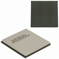
EP3SL150F1152C2N Altera, EP3SL150F1152C2N Datasheet - Page 174

EP3SL150F1152C2N
Manufacturer Part Number
EP3SL150F1152C2N
Description
IC STRATX III FPGA 150K 1152FBGA
Manufacturer
Altera
Series
Stratix® IIIr
Datasheets
1.EP3SL150F780C4N.pdf
(16 pages)
2.EP3SL150F780C4N.pdf
(332 pages)
3.EP3SL150F780C4N.pdf
(456 pages)
Specifications of EP3SL150F1152C2N
Number Of Logic Elements/cells
142500
Number Of Labs/clbs
5700
Total Ram Bits
6390
Number Of I /o
744
Voltage - Supply
0.86 V ~ 1.15 V
Mounting Type
Surface Mount
Operating Temperature
0°C ~ 85°C
Package / Case
1152-FBGA
For Use With
544-2568 - KIT DEVELOPMENT STRATIX III
Lead Free Status / RoHS Status
Lead free / RoHS Compliant
Number Of Gates
-
Other names
544-2409
EP3SL150F1152C2NES
EP3SL150F1152C2NES
Available stocks
Company
Part Number
Manufacturer
Quantity
Price
Part Number:
EP3SL150F1152C2N
Manufacturer:
ALTERA
Quantity:
20 000
- Current page: 174 of 456
- Download datasheet (7Mb)
6–26
Table 6–13. PLL Output Signals (Part 2 of 2)
Clock Feedback Modes
Stratix III Device Handbook, Volume 1
scandone
phasedone
fbout
Port
1
Stratix III PLLs support up to six different clock feedback modes. Each mode allows
clock multiplication and division, phase shifting, and programmable duty cycle.
Table 6–14
Table 6–14. Clock Feedback Mode Availability
The input and output delays are fully compensated by a PLL only when they are
using the dedicated clock input pins associated with a given PLL as the clock source.
Input and output delays are not compensated when cascading two adjacent top or
bottom PLLs even if they are using dedicated routing for cascading. For example,
when using PLL_T1 in normal mode, the clock delays from the input pin to the PLL
clock output-to-destination register are fully compensated provided the clock input
pin is one of the following four pins: CLK12, CLK13, CLK14, or CLK15. When an
RCLK or GCLK network drives the PLL, the input and output delays may not be fully
compensated in the Quartus II software.
Source-synchronous mode
No-compensation mode
Normal mode
Zero-delay buffer (ZDB) mode
External feedback mode
LVDS compensation
Notes to
(1) External feedback mode supported for single-ended inputs and outputs only on Left/Right PLLs.
(2) High-bandwidth PLL settings are not supported in external feedback mode. Select a "low" or "medium" PLL
(3) Differential HSTL and SSTL I/O standards are not supported in Top/Bottom PLLs for external feedback mode.
Clock Feedback Mode
bandwidth in the ALTPLL MegaWizard
Table
Signal indicating when the PLL has
completed reconfiguration.
One-to-0 transition indicates that
the PLL has been reconfigured.
When asserted it indicates that the
phase reconfiguration is complete
and the PLL is ready to act on a
possible second reconfiguration.
Asserts based on internal PLL
timing. De-asserts on rising edge of
SCANCLK.
Output of m counter. Used for clock
delay compensation.
lists the clock feedback modes supported by Stratix III PLLs.
6–14:
Description
(2)
TM
Plug-in Manager when using PLLs in external feedback mode.
Top/Bottom PLLs
Yes
Yes
Yes
Yes
Yes
No
Chapter 6: Clock Networks and PLLs in Stratix III Devices
(3)
PLL scan chain
PLL scan chain
M counter
Source
Availability
© July 2010 Altera Corporation
Left/Right PLLs
PLLs in Stratix III Devices
Destination
Yes
Logic array
Logic array
Logic array
Yes
Yes
Yes
Yes
Yes
(1)
Related parts for EP3SL150F1152C2N
Image
Part Number
Description
Manufacturer
Datasheet
Request
R

Part Number:
Description:
CYCLONE II STARTER KIT EP2C20N
Manufacturer:
Altera
Datasheet:

Part Number:
Description:
CPLD, EP610 Family, ECMOS Process, 300 Gates, 16 Macro Cells, 16 Reg., 16 User I/Os, 5V Supply, 35 Speed Grade, 24DIP
Manufacturer:
Altera Corporation
Datasheet:

Part Number:
Description:
CPLD, EP610 Family, ECMOS Process, 300 Gates, 16 Macro Cells, 16 Reg., 16 User I/Os, 5V Supply, 15 Speed Grade, 24DIP
Manufacturer:
Altera Corporation
Datasheet:

Part Number:
Description:
Manufacturer:
Altera Corporation
Datasheet:

Part Number:
Description:
CPLD, EP610 Family, ECMOS Process, 300 Gates, 16 Macro Cells, 16 Reg., 16 User I/Os, 5V Supply, 30 Speed Grade, 24DIP
Manufacturer:
Altera Corporation
Datasheet:

Part Number:
Description:
High-performance, low-power erasable programmable logic devices with 8 macrocells, 10ns
Manufacturer:
Altera Corporation
Datasheet:

Part Number:
Description:
High-performance, low-power erasable programmable logic devices with 8 macrocells, 7ns
Manufacturer:
Altera Corporation
Datasheet:

Part Number:
Description:
Classic EPLD
Manufacturer:
Altera Corporation
Datasheet:

Part Number:
Description:
High-performance, low-power erasable programmable logic devices with 8 macrocells, 10ns
Manufacturer:
Altera Corporation
Datasheet:

Part Number:
Description:
Manufacturer:
Altera Corporation
Datasheet:

Part Number:
Description:
Manufacturer:
Altera Corporation
Datasheet:

Part Number:
Description:
Manufacturer:
Altera Corporation
Datasheet:

Part Number:
Description:
CPLD, EP610 Family, ECMOS Process, 300 Gates, 16 Macro Cells, 16 Reg., 16 User I/Os, 5V Supply, 25 Speed Grade, 24DIP
Manufacturer:
Altera Corporation
Datasheet:


