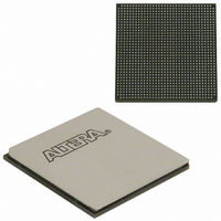
EP3SL150F1152C2N Altera, EP3SL150F1152C2N Datasheet - Page 168

EP3SL150F1152C2N
Manufacturer Part Number
EP3SL150F1152C2N
Description
IC STRATX III FPGA 150K 1152FBGA
Manufacturer
Altera
Series
Stratix® IIIr
Datasheets
1.EP3SL150F780C4N.pdf
(16 pages)
2.EP3SL150F780C4N.pdf
(332 pages)
3.EP3SL150F780C4N.pdf
(456 pages)
Specifications of EP3SL150F1152C2N
Number Of Logic Elements/cells
142500
Number Of Labs/clbs
5700
Total Ram Bits
6390
Number Of I /o
744
Voltage - Supply
0.86 V ~ 1.15 V
Mounting Type
Surface Mount
Operating Temperature
0°C ~ 85°C
Package / Case
1152-FBGA
For Use With
544-2568 - KIT DEVELOPMENT STRATIX III
Lead Free Status / RoHS Status
Lead free / RoHS Compliant
Number Of Gates
-
Other names
544-2409
EP3SL150F1152C2NES
EP3SL150F1152C2NES
Available stocks
Company
Part Number
Manufacturer
Quantity
Price
Part Number:
EP3SL150F1152C2N
Manufacturer:
ALTERA
Quantity:
20 000
- Current page: 168 of 456
- Download datasheet (7Mb)
6–20
Figure 6–18. Stratix III PLL Locations
Stratix III PLL Hardware Overview
Stratix III Device Handbook, Volume 1
Left/Right PLLs
Left/Right PLLs
PLL_L1_CLK
PLL_L4_CLK
CLK[0..3]
Figure 6–18
Stratix III devices contain up to 12 PLLs with advanced clock management features.
The main goal of a PLL is to synchronize the phase and frequency of an internal or
external clock to an input reference clock. There are a number of components that
comprise a PLL to achieve this phase alignment.
Stratix III PLLs align the rising edge of the input reference clock to a feedback clock
using the phase-frequency detector (PFD). The falling edges are determined by the
duty-cycle specifications. The PFD produces an up or down signal that determines
whether the voltage-controlled oscillator (VCO) needs to operate at a higher or lower
frequency. The output of the PFD feeds the charge pump and loop filter, which
produces a control voltage for setting the VCO frequency. If the PFD produces an up
signal, then the VCO frequency increases. A down signal decreases the VCO
frequency. The PFD outputs these up and down signals to a charge pump. If the
charge pump receives an up signal, current is driven into the loop filter. Conversely, if
the charge pump receives a down signal, current is drawn from the loop filter.
L1
L2
L3
L4
shows the location of the PLLs in Stratix III devices.
Top/Bottom PLLs
Top/Bottom PLLs
CLK[12..15]
CLK[4..7]
Q1
Q4
B1 B2
T1
T2
Q2
Q3
Top/Bottom PLLs
Top/Bottom PLLs
Chapter 6: Clock Networks and PLLs in Stratix III Devices
R1
R2
R3
R4
PLL_R1_CLK
CLK[8..11]
PLL-R4_CLK
© July 2010 Altera Corporation
PLLs in Stratix III Devices
Left/Right PLLs
Left/Right PLLs
Related parts for EP3SL150F1152C2N
Image
Part Number
Description
Manufacturer
Datasheet
Request
R

Part Number:
Description:
CYCLONE II STARTER KIT EP2C20N
Manufacturer:
Altera
Datasheet:

Part Number:
Description:
CPLD, EP610 Family, ECMOS Process, 300 Gates, 16 Macro Cells, 16 Reg., 16 User I/Os, 5V Supply, 35 Speed Grade, 24DIP
Manufacturer:
Altera Corporation
Datasheet:

Part Number:
Description:
CPLD, EP610 Family, ECMOS Process, 300 Gates, 16 Macro Cells, 16 Reg., 16 User I/Os, 5V Supply, 15 Speed Grade, 24DIP
Manufacturer:
Altera Corporation
Datasheet:

Part Number:
Description:
Manufacturer:
Altera Corporation
Datasheet:

Part Number:
Description:
CPLD, EP610 Family, ECMOS Process, 300 Gates, 16 Macro Cells, 16 Reg., 16 User I/Os, 5V Supply, 30 Speed Grade, 24DIP
Manufacturer:
Altera Corporation
Datasheet:

Part Number:
Description:
High-performance, low-power erasable programmable logic devices with 8 macrocells, 10ns
Manufacturer:
Altera Corporation
Datasheet:

Part Number:
Description:
High-performance, low-power erasable programmable logic devices with 8 macrocells, 7ns
Manufacturer:
Altera Corporation
Datasheet:

Part Number:
Description:
Classic EPLD
Manufacturer:
Altera Corporation
Datasheet:

Part Number:
Description:
High-performance, low-power erasable programmable logic devices with 8 macrocells, 10ns
Manufacturer:
Altera Corporation
Datasheet:

Part Number:
Description:
Manufacturer:
Altera Corporation
Datasheet:

Part Number:
Description:
Manufacturer:
Altera Corporation
Datasheet:

Part Number:
Description:
Manufacturer:
Altera Corporation
Datasheet:

Part Number:
Description:
CPLD, EP610 Family, ECMOS Process, 300 Gates, 16 Macro Cells, 16 Reg., 16 User I/Os, 5V Supply, 25 Speed Grade, 24DIP
Manufacturer:
Altera Corporation
Datasheet:


