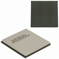
EP3SL150F1152C2N Altera, EP3SL150F1152C2N Datasheet - Page 284

EP3SL150F1152C2N
Manufacturer Part Number
EP3SL150F1152C2N
Description
IC STRATX III FPGA 150K 1152FBGA
Manufacturer
Altera
Series
Stratix® IIIr
Datasheets
1.EP3SL150F780C4N.pdf
(16 pages)
2.EP3SL150F780C4N.pdf
(332 pages)
3.EP3SL150F780C4N.pdf
(456 pages)
Specifications of EP3SL150F1152C2N
Number Of Logic Elements/cells
142500
Number Of Labs/clbs
5700
Total Ram Bits
6390
Number Of I /o
744
Voltage - Supply
0.86 V ~ 1.15 V
Mounting Type
Surface Mount
Operating Temperature
0°C ~ 85°C
Package / Case
1152-FBGA
For Use With
544-2568 - KIT DEVELOPMENT STRATIX III
Lead Free Status / RoHS Status
Lead free / RoHS Compliant
Number Of Gates
-
Other names
544-2409
EP3SL150F1152C2NES
EP3SL150F1152C2NES
Available stocks
Company
Part Number
Manufacturer
Quantity
Price
Part Number:
EP3SL150F1152C2N
Manufacturer:
ALTERA
Quantity:
20 000
- Current page: 284 of 456
- Download datasheet (7Mb)
Figure 8–20. Stratix III IOE Input Registers
Notes to
(1) You can bypass each register block in this path.
(2) This is the 0-phase resynchronization clock (from the read-leveling delay chain).
(3) The input clock can be from the DQS logic block (whether the postamble circuitry is bypassed or not) or from a global clock line.
(4) This input clock comes from the CQn logic block.
(5) This resynchronization clock can come either from the PLL or from the read-leveling delay chain.
(6) The I/O clock divider resides adjacent to the DQS logic block. In addition to the PLL and read-leveled resync clock, the I/O clock divider can also be fed by the DQS bus or CQn bus.
(7) The half-rate data and clock signals feed into a dual-port RAM in the FPGA core.
(8) You can dynamically change the dataoutbypass signal after configuration to select either the directin input or the output from the half data rate register to feed dataout.
(9) You must invert the strobe signal needs for DDR, DDR2, and DDR3 interfaces, except for QDR II or QDR II+ SRAM interfaces. This inversion is automatically done if you use the Altera external memory
(10) Each divider feeds up to six pins (from a × 4 DQS group) in the device. To feed wider DQS groups, you must chain multiple clock dividers together by feeding the slaveout output of one divider to the
(11) The bypass_output_register option allows you to select either the output from the second mux or the output of the fourth alignment/ synchronization register to feed dataout.
interface IPs.
masterin input of the neighboring pins’ divider.
Figure
8–20:
(Note 1)
Related parts for EP3SL150F1152C2N
Image
Part Number
Description
Manufacturer
Datasheet
Request
R

Part Number:
Description:
CYCLONE II STARTER KIT EP2C20N
Manufacturer:
Altera
Datasheet:

Part Number:
Description:
CPLD, EP610 Family, ECMOS Process, 300 Gates, 16 Macro Cells, 16 Reg., 16 User I/Os, 5V Supply, 35 Speed Grade, 24DIP
Manufacturer:
Altera Corporation
Datasheet:

Part Number:
Description:
CPLD, EP610 Family, ECMOS Process, 300 Gates, 16 Macro Cells, 16 Reg., 16 User I/Os, 5V Supply, 15 Speed Grade, 24DIP
Manufacturer:
Altera Corporation
Datasheet:

Part Number:
Description:
Manufacturer:
Altera Corporation
Datasheet:

Part Number:
Description:
CPLD, EP610 Family, ECMOS Process, 300 Gates, 16 Macro Cells, 16 Reg., 16 User I/Os, 5V Supply, 30 Speed Grade, 24DIP
Manufacturer:
Altera Corporation
Datasheet:

Part Number:
Description:
High-performance, low-power erasable programmable logic devices with 8 macrocells, 10ns
Manufacturer:
Altera Corporation
Datasheet:

Part Number:
Description:
High-performance, low-power erasable programmable logic devices with 8 macrocells, 7ns
Manufacturer:
Altera Corporation
Datasheet:

Part Number:
Description:
Classic EPLD
Manufacturer:
Altera Corporation
Datasheet:

Part Number:
Description:
High-performance, low-power erasable programmable logic devices with 8 macrocells, 10ns
Manufacturer:
Altera Corporation
Datasheet:

Part Number:
Description:
Manufacturer:
Altera Corporation
Datasheet:

Part Number:
Description:
Manufacturer:
Altera Corporation
Datasheet:

Part Number:
Description:
Manufacturer:
Altera Corporation
Datasheet:

Part Number:
Description:
CPLD, EP610 Family, ECMOS Process, 300 Gates, 16 Macro Cells, 16 Reg., 16 User I/Os, 5V Supply, 25 Speed Grade, 24DIP
Manufacturer:
Altera Corporation
Datasheet:


