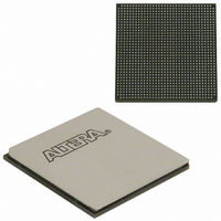
EP3SL150F1152C2N Altera, EP3SL150F1152C2N Datasheet - Page 277

EP3SL150F1152C2N
Manufacturer Part Number
EP3SL150F1152C2N
Description
IC STRATX III FPGA 150K 1152FBGA
Manufacturer
Altera
Series
Stratix® IIIr
Datasheets
1.EP3SL150F780C4N.pdf
(16 pages)
2.EP3SL150F780C4N.pdf
(332 pages)
3.EP3SL150F780C4N.pdf
(456 pages)
Specifications of EP3SL150F1152C2N
Number Of Logic Elements/cells
142500
Number Of Labs/clbs
5700
Total Ram Bits
6390
Number Of I /o
744
Voltage - Supply
0.86 V ~ 1.15 V
Mounting Type
Surface Mount
Operating Temperature
0°C ~ 85°C
Package / Case
1152-FBGA
For Use With
544-2568 - KIT DEVELOPMENT STRATIX III
Lead Free Status / RoHS Status
Lead free / RoHS Compliant
Number Of Gates
-
Other names
544-2409
EP3SL150F1152C2NES
EP3SL150F1152C2NES
Available stocks
Company
Part Number
Manufacturer
Quantity
Price
Part Number:
EP3SL150F1152C2N
Manufacturer:
ALTERA
Quantity:
20 000
- Current page: 277 of 456
- Download datasheet (7Mb)
Chapter 8: External Memory Interfaces in Stratix III Devices
Stratix III External Memory Interface Features
DQS Logic Block
Figure 8–13. Stratix III DQS Logic Block
Notes to
(1) The input reference clock for the DQS phase-shift circuitry can come from a PLL output clock or an input clock pin. For the exact PLL and input
(2) The dqsenable signal can also come from the Stratix III FPGA fabric.
© March 2010 Altera Corporation
DQS phase shift
settings from the
offsetctrlin [5:0]
settings from
Phase offset
shift circuitry
DQS phase-
DQS delay
clock pin location, refer to
circuitary
Figure
delayctrlin [5:0]
6
6
8–13:
DQS/CQ or
<dqs_offsetctrl_enable>
1
0
CQn Pin
6
D
Each DQS and CQn pin is connected to a separate DQS logic block, which consists of
the DQS delay chains, update enable circuitry, and DQS postamble circuitry, as shown
in
DQS Delay Chain
The DQS delay chains consist of a set of variable delay elements to allow the input
DQS/CQ and CQn signals to be shifted by the amount specified by the DQS
phase-shift circuitry or the logic array. There are four delay elements in the DQS delay
chain; the first delay chain closest to the DQS/CQ pin can either be shifted by the
DQS delay settings or by the sum of the DQS delay setting and the phase-offset
setting. The number of delay chains required is transparent because the
ALTMEMPHY megafunction automatically sets it when you choose the operating
frequency. The DQS delay settings can come from the DQS phase-shift circuitry on
either end of the I/O banks or from the logic array.
Delay elements in the DQS logic block have the same characteristics as the delay
elements in the DLL. When the DLL is not used to control the DQS delay chains, you
can input your own Gray-coded 6-bit or 5-bit settings using the
dqs_delayctrlin[5..0]signals available in the ALTMEMPHY megafunction.
These settings control 1, 2, 3, or all 4 delay elements in the DQS delay chains. The
ALTMEMPHY megafunction can also dynamically choose the number of DQS delay
chains required for the system. The amount of delay is equal to the sum of the delay
element’s intrinsic delay and the product of the number of delay steps and the value
of the delay steps.
Input Reference
Q
Bypass
Table 8–6
Figure
6
Clock (1)
0
1
dqsin
DQS Delay Chain
6
8–13.
through
D
Q
dqsupdateen
Table
6
0
1
<dqs_ctrl_latches_enable>
6
8–9.
Update
Circuitry
Enable
Resynchronization
phasectrlin[2:0]
Postam
Enable
Clock
ble
1xx
000
001
010
011
dqsenablein
dqsbusout
clk
DQS Enable Control
DQS Enable
dqsin
enaphasetransferreg
<level_dqs_enable>
0
1
delayctrlin
Stratix III Device Handbook, Volume 1
0
1
dqsbusout
6
DQS bus
postamble control clock
phasectrlin
<delay_dqs_enable_by_half_cycle>
0111
0110
0101
0100
0011
0010
0001
0000
Q
4
PRE
phaseinvertctrl
dqsenable (2)
D
0
1
0
1
dqsenableout
8–29
Related parts for EP3SL150F1152C2N
Image
Part Number
Description
Manufacturer
Datasheet
Request
R

Part Number:
Description:
CYCLONE II STARTER KIT EP2C20N
Manufacturer:
Altera
Datasheet:

Part Number:
Description:
CPLD, EP610 Family, ECMOS Process, 300 Gates, 16 Macro Cells, 16 Reg., 16 User I/Os, 5V Supply, 35 Speed Grade, 24DIP
Manufacturer:
Altera Corporation
Datasheet:

Part Number:
Description:
CPLD, EP610 Family, ECMOS Process, 300 Gates, 16 Macro Cells, 16 Reg., 16 User I/Os, 5V Supply, 15 Speed Grade, 24DIP
Manufacturer:
Altera Corporation
Datasheet:

Part Number:
Description:
Manufacturer:
Altera Corporation
Datasheet:

Part Number:
Description:
CPLD, EP610 Family, ECMOS Process, 300 Gates, 16 Macro Cells, 16 Reg., 16 User I/Os, 5V Supply, 30 Speed Grade, 24DIP
Manufacturer:
Altera Corporation
Datasheet:

Part Number:
Description:
High-performance, low-power erasable programmable logic devices with 8 macrocells, 10ns
Manufacturer:
Altera Corporation
Datasheet:

Part Number:
Description:
High-performance, low-power erasable programmable logic devices with 8 macrocells, 7ns
Manufacturer:
Altera Corporation
Datasheet:

Part Number:
Description:
Classic EPLD
Manufacturer:
Altera Corporation
Datasheet:

Part Number:
Description:
High-performance, low-power erasable programmable logic devices with 8 macrocells, 10ns
Manufacturer:
Altera Corporation
Datasheet:

Part Number:
Description:
Manufacturer:
Altera Corporation
Datasheet:

Part Number:
Description:
Manufacturer:
Altera Corporation
Datasheet:

Part Number:
Description:
Manufacturer:
Altera Corporation
Datasheet:

Part Number:
Description:
CPLD, EP610 Family, ECMOS Process, 300 Gates, 16 Macro Cells, 16 Reg., 16 User I/Os, 5V Supply, 25 Speed Grade, 24DIP
Manufacturer:
Altera Corporation
Datasheet:


