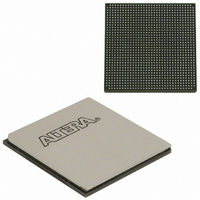
EP3SL150F1152C2N Altera, EP3SL150F1152C2N Datasheet - Page 300

EP3SL150F1152C2N
Manufacturer Part Number
EP3SL150F1152C2N
Description
IC STRATX III FPGA 150K 1152FBGA
Manufacturer
Altera
Series
Stratix® IIIr
Datasheets
1.EP3SL150F780C4N.pdf
(16 pages)
2.EP3SL150F780C4N.pdf
(332 pages)
3.EP3SL150F780C4N.pdf
(456 pages)
Specifications of EP3SL150F1152C2N
Number Of Logic Elements/cells
142500
Number Of Labs/clbs
5700
Total Ram Bits
6390
Number Of I /o
744
Voltage - Supply
0.86 V ~ 1.15 V
Mounting Type
Surface Mount
Operating Temperature
0°C ~ 85°C
Package / Case
1152-FBGA
For Use With
544-2568 - KIT DEVELOPMENT STRATIX III
Lead Free Status / RoHS Status
Lead free / RoHS Compliant
Number Of Gates
-
Other names
544-2409
EP3SL150F1152C2NES
EP3SL150F1152C2NES
Available stocks
Company
Part Number
Manufacturer
Quantity
Price
Part Number:
EP3SL150F1152C2N
Manufacturer:
ALTERA
Quantity:
20 000
- Current page: 300 of 456
- Download datasheet (7Mb)
9–6
Differential Receiver
Stratix III Device Handbook, Volume 1
f
You can bypass the Stratix III serializer to support DDR (×2) and SDR (×1) operations
to achieve a serialization factor of 2 and 1, respectively. The I/O element (IOE)
contains two data output registers that can each operate in either DDR or SDR mode.
The clock source for the registers in the IOE can come from any routing resource, from
the left/right PLL (PLL_Lx/PLL_Rx) or from the top/bottom (PLL_Tx/PLL_Bx) PLL.
Figure 9–4
Figure 9–4. Serializer Bypass for Stratix III Devices
For more information about how to use the differential transmitter, refer to the
ALTLVDS Megafunction User
The Stratix III device has dedicated circuitry to receive high-speed differential signals.
The receiver has a differential buffer, a shared PLL_Lx/PLL_Rx, DPA block,
synchronization FIFO buffer, data realignment block, and a deserializer. The
differential buffer can receive LVDS, mini-LVDS, and RSDS signal levels, which are
statically set in the Quartus II software Assignment Editor. The PLL receives the
external source clock input that is transmitted with the data and generates different
phases of the same clock. The DPA block chooses one of the clocks from the left/right
PLL and aligns the incoming data on each channel.
The synchronizer circuit is a 1-bit wide by 6-bit deep FIFO buffer that compensates for
any phase difference between the DPA clock and the data realignment block. If
necessary, the data realignment circuit can insert a single bit of latency in the serial bit
stream to align to the word boundary. The deserializer includes shift registers and
parallel load registers, and sends a maximum of 10 bits to the internal logic. The data
path in the Stratix III receiver is clocked by either a dffioclk signal or the DPA
recovered clock. The deserialization factor can be statically set to ×3, ×4, ×5, ×6, ×7, ×8,
×9, or ×10 with the Quartus II software. The left/right PLLs (PLL_Lx/PLL_Rx)
generate the load enable signal, which is derived from the deserialization factor
setting.
To support DDR (×2) or SDR (×1) operations, you can bypass the Stratix III
deserializer in MegaWizard Plug-In Manager in the Quartus II software. You cannot
use the DPA and the data realignment circuit when the deserializer is bypassed. The
IOE contains two data input registers that can operate in DDR or SDR mode. The
clock source for the registers in the IOE can come from any routing resource, from the
left/right PLLs or from the top/bottom PLLs.
Stratix III receiver.
shows the serializer bypass path.
Internal Logic
Chapter 9: High-Speed Differential I/O Interfaces and DPA in Stratix III Devices
Guide.
Serializer
IOE Supports SDR, DDR, or
Non-Registered Data Path
IOE
Figure 9–5
Not used (connection exists)
shows the block of the
© July 2010 Altera Corporation
Txclkout+
Txclkout–
Differential Receiver
Related parts for EP3SL150F1152C2N
Image
Part Number
Description
Manufacturer
Datasheet
Request
R

Part Number:
Description:
CYCLONE II STARTER KIT EP2C20N
Manufacturer:
Altera
Datasheet:

Part Number:
Description:
CPLD, EP610 Family, ECMOS Process, 300 Gates, 16 Macro Cells, 16 Reg., 16 User I/Os, 5V Supply, 35 Speed Grade, 24DIP
Manufacturer:
Altera Corporation
Datasheet:

Part Number:
Description:
CPLD, EP610 Family, ECMOS Process, 300 Gates, 16 Macro Cells, 16 Reg., 16 User I/Os, 5V Supply, 15 Speed Grade, 24DIP
Manufacturer:
Altera Corporation
Datasheet:

Part Number:
Description:
Manufacturer:
Altera Corporation
Datasheet:

Part Number:
Description:
CPLD, EP610 Family, ECMOS Process, 300 Gates, 16 Macro Cells, 16 Reg., 16 User I/Os, 5V Supply, 30 Speed Grade, 24DIP
Manufacturer:
Altera Corporation
Datasheet:

Part Number:
Description:
High-performance, low-power erasable programmable logic devices with 8 macrocells, 10ns
Manufacturer:
Altera Corporation
Datasheet:

Part Number:
Description:
High-performance, low-power erasable programmable logic devices with 8 macrocells, 7ns
Manufacturer:
Altera Corporation
Datasheet:

Part Number:
Description:
Classic EPLD
Manufacturer:
Altera Corporation
Datasheet:

Part Number:
Description:
High-performance, low-power erasable programmable logic devices with 8 macrocells, 10ns
Manufacturer:
Altera Corporation
Datasheet:

Part Number:
Description:
Manufacturer:
Altera Corporation
Datasheet:

Part Number:
Description:
Manufacturer:
Altera Corporation
Datasheet:

Part Number:
Description:
Manufacturer:
Altera Corporation
Datasheet:

Part Number:
Description:
CPLD, EP610 Family, ECMOS Process, 300 Gates, 16 Macro Cells, 16 Reg., 16 User I/Os, 5V Supply, 25 Speed Grade, 24DIP
Manufacturer:
Altera Corporation
Datasheet:


