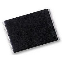
H27US08121B-TPCB HYNIX SEMICONDUCTOR, H27US08121B-TPCB Datasheet - Page 9

H27US08121B-TPCB
Manufacturer Part Number
H27US08121B-TPCB
Description
MEMORY, FLASH NAND 512MB, TSOP48
Manufacturer
HYNIX SEMICONDUCTOR
Datasheet
1.H27US08121B-TPCB.pdf
(43 pages)
Specifications of H27US08121B-TPCB
Memory Size
512Mbit
Access Time
45ns
Supply Voltage Range
2.7V To 3.6V
Memory Case Style
TSOP
No. Of Pins
48
Operating Temperature Range
0°C To +70°C
Package / Case
TSOP
Base Number
27
Memory Type
Flash - NAND
Memory Configuration
64M X 8, 32M X 16
Rohs Compliant
Yes
Lead Free Status / RoHS Status
Lead free / RoHS Compliant
Ready/Busy (RB)
The Ready/Busy output, RB, is an open-drain output that can be used to identify if the Program/ Erase/ Read (PER)
Controller is currently active.
When Ready/Busy is Low, V
Ready/Busy goes High, V
The use of an open-drain output allows the Ready/ Busy pins from several memories to be connected to a single pull-
up resistor. A Low will then indicate that one, or more, of the memories is busy.
Refer to the Ready/Busy Signal Electrical Characteristics section for details on how to calculate the value of the pull-up
resistor.
V
V
(read,program and erase).
An internal voltage detector disables all functions whenever V
devices) to protect the device from any involuntary program/erase during power-transitions.
Each device in a system should have V
to carry the required program and erase currents
V
Ground, V
BUS OPERATIONS
There are six standard bus operations that control the memory. Each of these is described in this section, see Tables 2,
Bus Operations, for a summary.
Command Input
Command Input bus operations are used to give commands to the memory. Command are accepted when Chip Enable
is Low, Command Latch Enable is High, Address Latch Enable is Low and Read Enable is High. They are latched on the
rising edge of the Write Enable signal.
Only I/O
Address Input
Address Input bus operations are used to input the memory address. Four bus cycles are required to input the
addresses for the 512Mb devices (refer to Tables 3 and 4, Address Insertion). The addresses are accepted when Chip
Enable is Low, Address Latch Enable is High, Command Latch Enable is Low and Read Enable is High. They are latched
on the rising edge of the Write Enable signal. Only I/O
See Figure 22 and Table 14 for details of the timings requirements.
Data Input
Data Input bus operations are used to input the data to be programmed.
Data is accepted only when Chip Enable is Low, Address Latch Enable is Low, Command Latch Enable is Low and Read
Enable is High. The data is latched on the rising edge of the Write Enable signal. The data is input sequentially using
the Write Enable signal.
See Figure 23 and Tables 14 and 15 for details of the timings requirements.
Rev 0.6 / Oct. 2004
CC
CC
SS
provides the power supply to the internal core of the memory device. It is the main power supply for all operations
Ground
Supply Voltage
0
SS
to I/O
, is the reference for the power supply. It must be connected to the system ground.
7
are used to input commands. See Figure 21 and Table 14 for details of the timings requirements.
OH
.
OL
, a read, program or erase operation is in progress. When the operation completes
CC
decoupled with a 0.1uF capacitor. The PCB track widths should be sufficient
512Mbit (64Mx8bit / 32Mx16bit) NAND Flash
0
to I/O
CC
7
are used to input addresses.
is below 2.5V (for 3V devices) or 1.5V (for 1.8V
HY27US(08/16)121M Series
HY27SS(08/16)121M Series
9


