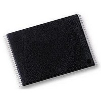
H27US08121B-TPCB HYNIX SEMICONDUCTOR, H27US08121B-TPCB Datasheet - Page 8

H27US08121B-TPCB
Manufacturer Part Number
H27US08121B-TPCB
Description
MEMORY, FLASH NAND 512MB, TSOP48
Manufacturer
HYNIX SEMICONDUCTOR
Datasheet
1.H27US08121B-TPCB.pdf
(43 pages)
Specifications of H27US08121B-TPCB
Memory Size
512Mbit
Access Time
45ns
Supply Voltage Range
2.7V To 3.6V
Memory Case Style
TSOP
No. Of Pins
48
Operating Temperature Range
0°C To +70°C
Package / Case
TSOP
Base Number
27
Memory Type
Flash - NAND
Memory Configuration
64M X 8, 32M X 16
Rohs Compliant
Yes
Lead Free Status / RoHS Status
Lead free / RoHS Compliant
SIGNAL DESCRIPTIONS
See Figure 1, Logic Diagram and Table 1, Signal Names, for a brief overview of the signals connected to this device.
Inputs/Outputs (I/O
Input/Outputs 0 to 7 are used to input the selected address, output the data during a Read opertion or input a com-
mand or data during a Write operation. The inputs are latched on the rising edge of Write Enable. I/O
floating when the device is deselected or the outputs are disabled.
Inputs/Outputs (I/O
Input/Outputs 8 to 15 are only available in x16 devices. They are used to output the data during a Read operation or
input data during a Write operation. Command and Address Inputs only require I/O
The inputs are latched on the rising edge of Write Enable. I/O
or the outputs are disabled.
Address Latch Enable (ALE)
The Address Latch Enable activates the latching of the Address inputs in the Command Interface. When ALE is high,
the inputs are latched on the rising edge of Write Enable.
Command Latch Enable (CLE)
The Command Latch Enable activates the latching of the Command inputs in the Command Interface. When CLE is
high, the inputs are latched on the rising edge of Write Enable.
Chip Enable (CE)
The Chip Enable input activates the memory control logic, input buffers, decoders and sense amplifiers. When Chip En-
able is low, V
lected and does not go into standby mode.
When the device is executing a Sequential Row Read operation, Chip Enable must be held low (from the second page
read onwards) during the time that the device is busy (t
aborted.
Read Enable (RE)
The Read Enable, RE, controls the sequential data output during Read operations. Data is valid t
edge of RE. The falling edge of RE also increments the internal column address counter by one.
Write Enable (WE). The Write Enable input, WE, controls writing to the Command Interface, Input Address and Data
latches. Both addresses and data are latched on the rising edge of Write Enable.
During power-up and power-down a recovery time of 1us (min) is required before the Command Interface is ready to
accept a command. It is recommended to keep Write Enable high during the recovery time.
Write Protect (WP).
The Write Protect pin is an input that gives a hardware protection against unwanted program or erase operations.
When Write Protect is Low, V
It is recommended to keep the Write Protect pin Low, V
Rev 0.6 / Oct. 2004
IL
, the device is selected. If Chip Enable goes high, V
0
8
-I/O
-I/O
IL
7
15
, the device does not accept any program or erase operations.
)
)
512Mbit (64Mx8bit / 32Mx16bit) NAND Flash
BLBH1
IL
, during power-up and power-down.
). If Chip Enable goes high during t
8
-I/O
15
IH
can be left floating when the device is deselected
, while the device is busy, the device remains se-
HY27US(08/16)121M Series
HY27SS(08/16)121M Series
0
to I/O
7
.
BLBH1
RLQV
0
-I/O
after the falling
the operation is
7
can be left
8


