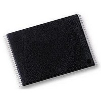
H27US08121B-TPCB HYNIX SEMICONDUCTOR, H27US08121B-TPCB Datasheet - Page 19

H27US08121B-TPCB
Manufacturer Part Number
H27US08121B-TPCB
Description
MEMORY, FLASH NAND 512MB, TSOP48
Manufacturer
HYNIX SEMICONDUCTOR
Datasheet
1.H27US08121B-TPCB.pdf
(43 pages)
Specifications of H27US08121B-TPCB
Memory Size
512Mbit
Access Time
45ns
Supply Voltage Range
2.7V To 3.6V
Memory Case Style
TSOP
No. Of Pins
48
Operating Temperature Range
0°C To +70°C
Package / Case
TSOP
Base Number
27
Memory Type
Flash - NAND
Memory Configuration
64M X 8, 32M X 16
Rohs Compliant
Yes
Lead Free Status / RoHS Status
Lead free / RoHS Compliant
Once the erase operation has completed the Status Register can be checked for errors.
Reset
The Reset command is used to reset the Command Interface and Status Register. If the Reset command is issued dur-
ing any operation, the operation will be aborted. If it was a program or erase operation that was aborted, the contents
of the memory locations being modified will no longer be valid as the data will be partially programmed or erased.
If the device has already been reset then the new Reset command will not be accepted. The Ready/Busy signal goes
Low for t
performing when the command was issued, refer to Table 15 for the values.
Read Status Register
The device contains a Status Register which provides information on the current or previous Program or Erase opera-
tion. The various bits in the Status Register convey information and errors on the operation.
The Status Register is read by issuing the Read Status Register command. The Status Register information is present
on the output data bus (I/O
several memories are connected in a system, the use of Chip Enable and Read Enable signals allows the system to poll
each device separately, even when the Ready/Busy pins are common-wired. It is not necessary to toggle the Chip
Enable or Read Enable signals to update the contents of the Status Register.
After the Read Status Register command has been issued, the device remains in Read Status Register mode until
another command is issued. Therefore if a Read Status Register command is issued during a Random Read cycle a
new read command must be issued to continue with a Page Read or Sequential Row Read operation.
The Status Register bits are summarized in Table 6, Status Register Bits. Refer to Table 6 in conjunction with the fol-
lowing text descriptions.
Write Protection Bit (SR7)
The Write Protection bit can be used to identify if the device is protected or not. If the Write Protection bit is set to '1'
the device is not protected and program or erase operations are allowed. If the Write Protection bit is set to '0' the
device is protected and program or erase operations are not allowed.
Rev 0.6 / Oct. 2004
I/O
RB
Block Erase
Setup Code
BLBH4
60h
after the Reset command is issued. The value of t
Block Address
0
- I/O
Inputs
7
) on the falling edge of Chip Enable or Read Enable, whichever occurs last. When
Figure 17. Block Erase Operation
Confirm
512Mbit (64Mx8bit / 32Mx16bit) NAND Flash
Code
D0h
BLBH4
(Erase Busy time)
depends on the operation that the device was
HY27US(08/16)121M Series
tBLBH3
HY27SS(08/16)121M Series
Busy
Read Status Register
70h
SR0
19


