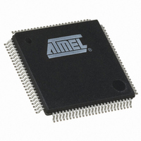
ATSAM3S4CA-AU Atmel, ATSAM3S4CA-AU Datasheet - Page 851

ATSAM3S4CA-AU
Manufacturer Part Number
ATSAM3S4CA-AU
Description
IC MCU 32BIT 256KB FLASH 100LQFP
Manufacturer
Atmel
Series
SAM3Sr
Specifications of ATSAM3S4CA-AU
Core Processor
ARM® Cortex-M3™
Core Size
32-Bit
Speed
64MHz
Connectivity
EBI/EMI, I²C, MMC, SPI, SSC, UART/USART, USB
Peripherals
Brown-out Detect/Reset, DMA, I²S, POR, PWM, WDT
Number Of I /o
79
Program Memory Size
256KB (256K x 8)
Program Memory Type
FLASH
Ram Size
48K x 8
Voltage - Supply (vcc/vdd)
1.62 V ~ 1.95 V
Data Converters
A/D 16x10/12b, D/A 2x12b
Oscillator Type
Internal
Operating Temperature
-40°C ~ 85°C
Package / Case
100-LQFP
Controller Family/series
ATSAM3S
No. Of I/o's
79
Ram Memory Size
48KB
Cpu Speed
64MHz
No. Of Timers
6
Rohs Compliant
Yes
Processor Series
ATSAM3x
Core
ARM Cortex M3
3rd Party Development Tools
JTRACE-CM3, MDK-ARM, RL-ARM, ULINK2
Development Tools By Supplier
ATSAM3S-EK
Cpu Family
AT91
Device Core
ARM Cortex-M3
Device Core Size
32b
Frequency (max)
64MHz
Total Internal Ram Size
48KB
# I/os (max)
79
Number Of Timers - General Purpose
6
Operating Supply Voltage (typ)
1.8/3.3V
Operating Supply Voltage (max)
1.95/3.6V
Operating Supply Voltage (min)
1.62V
On-chip Adc
16-chx12-bit
On-chip Dac
2-chx12-bit
Instruction Set Architecture
RISC
Operating Temp Range
-40C to 85C
Operating Temperature Classification
Industrial
Mounting
Surface Mount
Pin Count
100
Package Type
LQFP
Lead Free Status / RoHS Status
Lead free / RoHS Compliant
Eeprom Size
-
Lead Free Status / Rohs Status
Details
Available stocks
Company
Part Number
Manufacturer
Quantity
Price
Part Number:
ATSAM3S4CA-AU
Manufacturer:
ATMEL/爱特梅尔
Quantity:
20 000
- Current page: 851 of 1118
- Download datasheet (24Mb)
36.6.2.2
6500C–ATARM–8-Feb-11
Comparator
The comparator continuously compares its counter value with the channel period defined by
CPRD in the
defined by CDTY in the
generate an output signal OCx accordingly.
The different properties of the waveform of the output OCx are:
• the clock selection. The channel counter is clocked by one of the clocks provided by the
• the waveform period. This channel parameter is defined in the CPRD field of the
• the waveform duty-cycle. This channel parameter is defined in the CDTY field of the
clock generator described in the previous section. This channel parameter is defined in the
CPRE field of the
reset at 0.
PWM_CPRDx register.
If the waveform is left aligned, then the output waveform period depends on the counter
source clock and can be calculated:
By using the PWM master clock (MCK) divided by an X given prescaler value (with X being 1,
2, 4, 8, 16, 32, 64, 128, 256, 512, or 1024), the resulting period formula will be:
By using the PWM master clock (MCK) divided by one of both DIVA or DIVB divider, the
formula becomes, respectively:
If the waveform is center aligned then the output waveform period depends on the counter
source clock and can be calculated:
By using the PWM master clock (MCK) divided by an X given prescaler value
(with X being 1, 2, 4, 8, 16, 32, 64, 128, 256, 512, or 1024). The resulting period formula will
be:
By using the PWM master clock (MCK) divided by one of both DIVA or DIVB divider, the
formula becomes, respectively:
PWM_CDTYx register.
If the waveform is left aligned then:
If the waveform is center aligned, then:
(
------------------------------- -
(
------------------------------------------ -
(
------------------------------------------ -
(
----------------------------------------------------- -
X
CRPD
2
2
duty cycle
duty cycle
×
×
×
MCK
X
CPRD
CPRD
MCK
MCK
×
MCK
×
CPRD
DIVA
“PWM Channel Period Register” on page 920
)
×
=
DIVA
=
)
)
(
----------------------------------------------------------------------------------------------------------- -
(
----------------------------------------------------------------------------------------------------------------------------- -
period 1
or
(
period
“PWM Channel Mode Register” on page 916
)
(
------------------------------------------ -
or
CRPD
“PWM Channel Duty Cycle Register” on page 918
(
----------------------------------------------------- -
–
2
⁄
MCK
×
2
×
⁄
CPRD
) 1
DIVB
fchannel_x_clock
–
MCK
period
⁄
(
×
)
period
fchannel_x_clock
DIVB
)
⁄
2
)
×
CDTY
×
CDTY
)
SAM3S Preliminary
(PWM_CPRDx) and the duty-cycle
) )
(PWM_CMRx). This field is
(PWM_CDTYx) to
851
Related parts for ATSAM3S4CA-AU
Image
Part Number
Description
Manufacturer
Datasheet
Request
R

Part Number:
Description:
KIT EVAL FOR ATSAM3S4C
Manufacturer:
Atmel
Datasheet:

Part Number:
Description:
Development Boards & Kits - ARM EVAL KIT SAM3S8 & SAM3SD8 series
Manufacturer:
Atmel
Datasheet:

Part Number:
Description:
AT91 ARM Cortex M3-based Processor
Manufacturer:
ATMEL [ATMEL Corporation]
Datasheet:

Part Number:
Description:
DEV KIT FOR AVR/AVR32
Manufacturer:
Atmel
Datasheet:

Part Number:
Description:
INTERVAL AND WIPE/WASH WIPER CONTROL IC WITH DELAY
Manufacturer:
ATMEL Corporation
Datasheet:

Part Number:
Description:
Low-Voltage Voice-Switched IC for Hands-Free Operation
Manufacturer:
ATMEL Corporation
Datasheet:

Part Number:
Description:
MONOLITHIC INTEGRATED FEATUREPHONE CIRCUIT
Manufacturer:
ATMEL Corporation
Datasheet:

Part Number:
Description:
AM-FM Receiver IC U4255BM-M
Manufacturer:
ATMEL Corporation
Datasheet:

Part Number:
Description:
Monolithic Integrated Feature Phone Circuit
Manufacturer:
ATMEL Corporation
Datasheet:

Part Number:
Description:
Multistandard Video-IF and Quasi Parallel Sound Processing
Manufacturer:
ATMEL Corporation
Datasheet:

Part Number:
Description:
High-performance EE PLD
Manufacturer:
ATMEL Corporation
Datasheet:

Part Number:
Description:
8-bit Flash Microcontroller
Manufacturer:
ATMEL Corporation
Datasheet:


